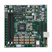
LFE3-95E-PCIE-DKN Lattice, LFE3-95E-PCIE-DKN Datasheet - Page 110

LFE3-95E-PCIE-DKN
Manufacturer Part Number
LFE3-95E-PCIE-DKN
Description
MCU, MPU & DSP Development Tools LatticeECP3 PCI Express Dev Kit
Manufacturer
Lattice
Datasheet
1.LFE3-150EA-7FN672CTW.pdf
(130 pages)
Specifications of LFE3-95E-PCIE-DKN
Processor To Be Evaluated
LFE3-95EA-x
Processor Series
LatticeECP3
Interface Type
SPI
Operating Supply Voltage
1.2 V to 3.3 V
Lead Free Status / RoHS Status
Lead free / RoHS Compliant
Signal Descriptions
March 2010
© 2010 Lattice Semiconductor Corp. All Lattice trademarks, registered trademarks, patents, and disclaimers are as listed at www.latticesemi.com/legal. All other brand
or product names are trademarks or registered trademarks of their respective holders. The specifications and information herein are subject to change without notice.
www.latticesemi.com
General Purpose
P[Edge] [Row/Column Number]_[A/B]
P[Edge][Row Number]E_[A/B/C/D]
GSRN
NC
RESERVED
GND
V
V
V
V
V
V
VTTx
XRES
PLL, DLL and Clock Functions
[LOC][num]_GPLL[T, C]_IN_[index]
[LOC][num]_GPLL[T, C]_FB_[index]
[LOC]0_GDLLT_IN_[index]
[LOC]0_GDLLT_FB_[index]
PCLK[T, C][n:0]_[3:0]
CC
CCAUX
CCIOx
CCA
CCPLL_[LOC]
REF1_x
1
, V
REF2_x
Signal Name
I/O
I/O
I/O
I/O
—
—
—
—
—
—
—
—
—
—
—
I
I
I
I
I
[Edge] indicates the edge of the device on which the pad is located. Valid
edge designations are L (Left), B (Bottom), R (Right), T (Top).
[Row/Column Number] indicates the PFU row or the column of the device on
which the PIC exists. When Edge is T (Top) or B (Bottom), only need to spec-
ify Column Number. When Edge is L (Left) or R (Right), only need to specify
Row Number.
[A/B] indicates the PIO within the PIC to which the pad is connected. Some of
these user-programmable pins are shared with special function pins. These
pins, when not used as special purpose pins, can be programmed as I/Os for
user logic. During configuration the user-programmable I/Os are tri-stated
with an internal pull-up resistor enabled. If any pin is not used (or not bonded
to a package pin), it is also tri-stated with an internal pull-up resistor enabled
after configuration.
These general purpose signals are input-only pins and are located near the
PLLs.
Global RESET signal (active low). Any I/O pin can be GSRN.
No connect.
This pin is reserved and should not be connected to anything on the board.
Ground. Dedicated pins.
Power supply pins for core logic. Dedicated pins.
Auxiliary power supply pin. This dedicated pin powers all the differential and
referenced input buffers.
Dedicated power supply pins for I/O bank x.
SERDES, transmit, receive, PLL and reference clock buffer power supply.
General purpose PLL supply pins where LOC=L (left) or R (right).
Reference supply pins for I/O bank x. Pre-determined pins in each bank are
assigned as V
Power supply for on-chip termination of I/Os (Required for DDR3 and LVDS at
1.25Gbps).
10K ohm +/-1% resistor must be connected between this pad and ground.
General Purpose PLL (GPLL) input pads: LUM, LLM, RUM, RLM, num = row
from center, T = true and C = complement, index A,B,C...at each side.
Optional feedback GPLL input pads: LUM, LLM, RUM, RLM, num = row from
center, T = true and C = complement, index A,B,C...at each side.
General Purpose DLL (GDLL) input pads where LOC=RUM or LUM, T is True
Complement, index is A or B.
Optional feedback GDLL input pads where LOC=RUM or LUM, T is True
Complement, index is A or B.
Primary Clock pads, T = true and C = complement, n per side, indexed by
bank and 0, 1, 2, 3 within bank.
LatticeECP3 Family Data Sheet
4-1
REF
inputs. When not used, they may be used as I/O pins.
Description
Pinout Information
DS1021
Preliminary Data Sheet DS1021
Pinout Information_01.2


