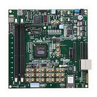
LFE3-95E-PCIE-DKN Lattice, LFE3-95E-PCIE-DKN Datasheet - Page 55

LFE3-95E-PCIE-DKN
Manufacturer Part Number
LFE3-95E-PCIE-DKN
Description
MCU, MPU & DSP Development Tools LatticeECP3 PCI Express Dev Kit
Manufacturer
Lattice
Datasheet
1.LFE3-150EA-7FN672CTW.pdf
(130 pages)
Specifications of LFE3-95E-PCIE-DKN
Processor To Be Evaluated
LFE3-95EA-x
Processor Series
LatticeECP3
Interface Type
SPI
Operating Supply Voltage
1.2 V to 3.3 V
Lead Free Status / RoHS Status
Lead free / RoHS Compliant
- Current page: 55 of 130
- Download datasheet (3Mb)
Lattice Semiconductor
DC Electrical Characteristics
I
I
I
I
I
I
I
I
V
C1
C2
1. Input or I/O leakage current is measured with the pin configured as an input or as an I/O with the output driver tri-stated. It is not measured
2. T
3. Applicable to general purpose I/Os in top and bottom banks.
4. When used as V
Symbol
IL
IH
PU
PD
BHLS
BHHS
BHLO
BHHO
BHT
, I
1, 3
with the output driver active. Bus maintenance circuits are disabled.
A
IH
25
1, 4
o
C, f = 1.0MHz.
Input or I/O Low Leakage
Input or I/O High Leakage
I/O Active Pull-up Current
I/O Active Pull-down Current
Bus Hold Low Sustaining Current V
Bus Hold High Sustaining Current V
Bus Hold Low Overdrive Current 0 V
Bus Hold High Overdrive Current 0 V
Bus Hold Trip Points
Dedicated Input Capacitance
I/O Capacitance
REF
, maximum leakage= 25µA.
Parameter
2
Over Recommended Operating Conditions
2
0 V
0 V
0 V
(V
V
V
V
V
V
IL
IN
IN
CCIO
CC
CCIO
CC
CCIO
(MAX) V
= V
= 0.7 V
= 1.2V, V
= 1.2V, V
IN
IN
IN
IN
IN
= 3.3V, 2.5V, 1.8V, 1.5V, 1.2V,
= 3.3V, 2.5V, 1.8V, 1.5V, 1.2V,
- 0.2V) < V
IL
(V
0.7 V
V
V
V
(MAX)
CCIO
CCIO
IH
CCIO
CCIO
(MAX)
IO
IO
Condition
IN
CCIO
3-3
= 0 to V
= 0 to V
V
- 0.2V)
IN
CCIO
3.6V
IH
IH
(MAX)
(MAX)
DC and Switching Characteristics
LatticeECP3 Family Data Sheet
V
IL
Min.
-30
-30
(MAX)
30
30
—
—
—
—
—
—
Typ.
—
—
—
—
—
—
—
—
—
8
6
V
IH
Max.
-210
-210
150
210
210
10
—
—
—
—
(MIN)
Units
µA
µA
µA
µA
µA
µA
µA
µA
pf
pf
V
Related parts for LFE3-95E-PCIE-DKN
Image
Part Number
Description
Manufacturer
Datasheet
Request
R

Part Number:
Description:
FPGA - Field Programmable Gate Array 92K LUTs, 490 I/O 8 Speed
Manufacturer:
Lattice

Part Number:
Description:
FPGA - Field Programmable Gate Array 92K LUTs, 380 I/O 7 Speed
Manufacturer:
Lattice

Part Number:
Description:
FPGA - Field Programmable Gate Array 92K LUTs, 295 I/O 7 Speed
Manufacturer:
Lattice

Part Number:
Description:
FPGA - Field Programmable Gate Array 92K LUTs, 380 I/O 6 Speed
Manufacturer:
Lattice

Part Number:
Description:
FPGA - Field Programmable Gate Array 92K LUTs, 490 I/O 6 Speed
Manufacturer:
Lattice

Part Number:
Description:
FPGA - Field Programmable Gate Array 92K LUTs, 295 I/O 8 Speed
Manufacturer:
Lattice

Part Number:
Description:
FPGA - Field Programmable Gate Array 92K LUTs, 490 I/O 8 Speed
Manufacturer:
Lattice

Part Number:
Description:
FPGA - Field Programmable Gate Array 92K LUTs, 380 I/O 8 Speed
Manufacturer:
Lattice

Part Number:
Description:
FPGA - Field Programmable Gate Array 92K LUTs, 490 I/O 6 Speed
Manufacturer:
Lattice

Part Number:
Description:
FPGA - Field Programmable Gate Array 92K LUTs, 295 I/O 6 Speed
Manufacturer:
Lattice

Part Number:
Description:
FPGA - Field Programmable Gate Array 92K LUTs, 490 I/O 7 Speed
Manufacturer:
Lattice

Part Number:
Description:
FPGA - Field Programmable Gate Array 92K LUTs, 295 I/O 8 Speed
Manufacturer:
Lattice

Part Number:
Description:
FPGA - Field Programmable Gate Array 92K LUTs, 490 I/O 7 Speed
Manufacturer:
Lattice

Part Number:
Description:
FPGA - Field Programmable Gate Array 92K LUTs, 380 I/O 6 Speed
Manufacturer:
Lattice

Part Number:
Description:
FPGA - Field Programmable Gate Array 92K LUTs, 295 I/O 7 Speed
Manufacturer:
Lattice


