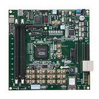
LFE3-95E-PCIE-DKN Lattice, LFE3-95E-PCIE-DKN Datasheet - Page 47

LFE3-95E-PCIE-DKN
Manufacturer Part Number
LFE3-95E-PCIE-DKN
Description
MCU, MPU & DSP Development Tools LatticeECP3 PCI Express Dev Kit
Manufacturer
Lattice
Datasheet
1.LFE3-150EA-7FN672CTW.pdf
(130 pages)
Specifications of LFE3-95E-PCIE-DKN
Processor To Be Evaluated
LFE3-95EA-x
Processor Series
LatticeECP3
Interface Type
SPI
Operating Supply Voltage
1.2 V to 3.3 V
Lead Free Status / RoHS Status
Lead free / RoHS Compliant
Lattice Semiconductor
Please see TN1177,
Equalization Filter
Equalization filtering is available for single-ended inputs on both true and complementary I/Os, and for differential
inputs on the true I/Os on the left, right, and top sides. Equalization is required to compensate for the difficulty of
sampling alternating logic transitions with a relatively slow slew rate. It is considered the most useful for the Input
DDRX2 modes, used in DDR3 memory, LVDS, or TRLVDS signaling. Equalization filter acts as a tunable filter with
settings to determine the level of correction. In the LatticeECP3 devices, there are four settings available: 0 (none),
1, 2 and 3. The default setting is 0. The equalization logic resides in the sysI/O buffers, the two bits of setting is set
uniquely in each input IOLOGIC block. Therefore, each sysI/O can have a unique equalization setting within a
DQS-12 group.
Hot Socketing
LatticeECP3 devices have been carefully designed to ensure predictable behavior during power-up and power-
down. During power-up and power-down sequences, the I/Os remain in tri-state until the power supply voltage is
high enough to ensure reliable operation. In addition, leakage into I/O pins is controlled within specified limits.
Please refer to the Hot Socketing Specifications in the DC and Switching Characteristics in this data sheet.
SERDES and PCS (Physical Coding Sublayer)
LatticeECP3 devices feature up to 16 channels of embedded SERDES/PCS arranged in quads at the bottom of the
devices supporting up to 3.2Gbps data rate. Figure 2-40 shows the position of the quad blocks for the LatticeECP3-
150 devices. Table 2-14 shows the location of available SERDES Quads for all devices.
The LatticeECP3 SERDES/PCS supports a range of popular serial protocols, including:
Each quad contains four dedicated SERDES for high speed, full duplex serial data transfer. Each quad also has a
PCS block that interfaces to the SERDES channels and contains protocol specific digital logic to support the stan-
dards listed above. The PCS block also contains interface logic to the FPGA fabric. All PCS logic for dedicated pro-
tocol support can also be bypassed to allow raw 8-bit or 10-bit interfaces to the FPGA fabric.
Even though the SERDES/PCS blocks are arranged in quads, multiple baud rates can be supported within a quad
with the use of dedicated, per channel 1, 2 and 11 rate dividers. Additionally, multiple quads can be arranged
together to form larger data pipes.
For information on how to use the SERDES/PCS blocks to support specific protocols, as well on how to combine
multiple protocols and baud rates within a device, please refer to TN1176,
Guide.
• PCI Express 1.1
• Ethernet (XAUI, GbE - 1000 Base CS/SX/LX and SGMII)
• Serial RapidIO
• SMPTE SDI (3G, HD, SD)
• CPRI
• SONET/SDH (STS-3, STS-12, STS-48)
LatticeECP3 sysIO Usage Guide
for on-chip termination usage and value ranges.
2-44
LatticeECP3 Family Data Sheet
LatticeECP3 SERDES/PCS Usage
Architecture


