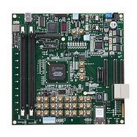
LFE3-95E-PCIE-DKN Lattice, LFE3-95E-PCIE-DKN Datasheet - Page 73

LFE3-95E-PCIE-DKN
Manufacturer Part Number
LFE3-95E-PCIE-DKN
Description
MCU, MPU & DSP Development Tools LatticeECP3 PCI Express Dev Kit
Manufacturer
Lattice
Datasheet
1.LFE3-150EA-7FN672CTW.pdf
(130 pages)
Specifications of LFE3-95E-PCIE-DKN
Processor To Be Evaluated
LFE3-95EA-x
Processor Series
LatticeECP3
Interface Type
SPI
Operating Supply Voltage
1.2 V to 3.3 V
Lead Free Status / RoHS Status
Lead free / RoHS Compliant
- Current page: 73 of 130
- Download datasheet (3Mb)
LatticeECP3 External Switching Characteristics (Continued)
Lattice Semiconductor
f
DDR3 (Using PLL for SCLK) I/O Pin Parameters
t
t
t
t
f
1. Commercial timing numbers are shown. Industrial numbers are typically slower and can be extracted from the ispLEVER software.
2. General I/O timing numbers based on LVCMOS 2.5, 12mA, 0pf load.
3. Generic DDR timing numbers based on LVDS I/O.
4. DDR timing numbers based on SSTL25. DDR2 timing numbers based on SSTL18.
5. DDR3 timing numbers based on SSTL15.
6. Uses LVDS I/O standard.
7. The current version of software does not support per bank skew numbers; this will be supported in a future release.
8. Maximum clock frequencies are tested under best case conditions. System performance may vary upon the user environment.
MAX_DDR2
DVADQ
DVEDQ
DQVBS
DQVAS
MAX_DDR3
Parameter
DDR2 Clock Frequency
Data Valid After DQS (DDR Read)
Data Hold After DQS (DDR Read)
Data Valid Before DQS
Data Valid After DQS
DDR3 clock frequency
Over Recommended Commercial Operating Conditions
Description
ECP3-70E/95E
ECP3-150EA
ECP3-150EA
ECP3-150EA
ECP3-150EA
ECP3-150EA
3-21
Device
Min.
0.64
0.25
0.25
133
266
—
DC and Switching Characteristics
-8
LatticeECP3 Family Data Sheet
0.225
Max.
266
400
—
—
—
Min.
0.64
0.25
0.25
133
266
—
-7
0.225
Max.
200
333
1, 2
—
—
—
Min.
0.64
0.25
0.25
133
266
—
-6
0.225
Max.
166
300
—
—
—
Units
MHz
MHz
UI
UI
UI
UI
Related parts for LFE3-95E-PCIE-DKN
Image
Part Number
Description
Manufacturer
Datasheet
Request
R

Part Number:
Description:
FPGA - Field Programmable Gate Array 92K LUTs, 490 I/O 8 Speed
Manufacturer:
Lattice

Part Number:
Description:
FPGA - Field Programmable Gate Array 92K LUTs, 380 I/O 7 Speed
Manufacturer:
Lattice

Part Number:
Description:
FPGA - Field Programmable Gate Array 92K LUTs, 295 I/O 7 Speed
Manufacturer:
Lattice

Part Number:
Description:
FPGA - Field Programmable Gate Array 92K LUTs, 380 I/O 6 Speed
Manufacturer:
Lattice

Part Number:
Description:
FPGA - Field Programmable Gate Array 92K LUTs, 490 I/O 6 Speed
Manufacturer:
Lattice

Part Number:
Description:
FPGA - Field Programmable Gate Array 92K LUTs, 295 I/O 8 Speed
Manufacturer:
Lattice

Part Number:
Description:
FPGA - Field Programmable Gate Array 92K LUTs, 490 I/O 8 Speed
Manufacturer:
Lattice

Part Number:
Description:
FPGA - Field Programmable Gate Array 92K LUTs, 380 I/O 8 Speed
Manufacturer:
Lattice

Part Number:
Description:
FPGA - Field Programmable Gate Array 92K LUTs, 490 I/O 6 Speed
Manufacturer:
Lattice

Part Number:
Description:
FPGA - Field Programmable Gate Array 92K LUTs, 295 I/O 6 Speed
Manufacturer:
Lattice

Part Number:
Description:
FPGA - Field Programmable Gate Array 92K LUTs, 490 I/O 7 Speed
Manufacturer:
Lattice

Part Number:
Description:
FPGA - Field Programmable Gate Array 92K LUTs, 295 I/O 8 Speed
Manufacturer:
Lattice

Part Number:
Description:
FPGA - Field Programmable Gate Array 92K LUTs, 490 I/O 7 Speed
Manufacturer:
Lattice

Part Number:
Description:
FPGA - Field Programmable Gate Array 92K LUTs, 380 I/O 6 Speed
Manufacturer:
Lattice

Part Number:
Description:
FPGA - Field Programmable Gate Array 92K LUTs, 295 I/O 7 Speed
Manufacturer:
Lattice


