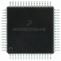
MC68SEC000AA16 Freescale Semiconductor, MC68SEC000AA16 Datasheet - Page 121

MC68SEC000AA16
Manufacturer Part Number
MC68SEC000AA16
Description
IC MPU 32BIT 16MHZ 64-QFP
Manufacturer
Freescale Semiconductor
Series
M68000r
Specifications of MC68SEC000AA16
Processor Type
M680x0 32-Bit
Speed
16MHz
Voltage
3.3V, 5V
Mounting Type
Surface Mount
Package / Case
64-QFP
Processor Series
M680xx
Core
CPU32
Maximum Clock Frequency
16 MHz
Operating Supply Voltage
3.3 V, 5 V
Maximum Operating Temperature
+ 105 C
Mounting Style
SMD/SMT
Minimum Operating Temperature
0 C
Core Size
32 Bit
Cpu Speed
16MHz
Digital Ic Case Style
QFP
No. Of Pins
64
Supply Voltage Range
5V
Operating Temperature Range
0°C To +70°C
Frequency Typ
20MHz
Filter Terminals
SMD
Rohs Compliant
Yes
Clock Frequency
16MHz
Lead Free Status / RoHS Status
Lead free / RoHS Compliant
Features
-
Lead Free Status / Rohs Status
Lead free / RoHS Compliant
Available stocks
Company
Part Number
Manufacturer
Quantity
Price
Company:
Part Number:
MC68SEC000AA16
Manufacturer:
Freescale Semiconductor
Quantity:
10 000
Part Number:
MC68SEC000AA16
Manufacturer:
FREESCALE
Quantity:
20 000
Company:
Part Number:
MC68SEC000AA16R2
Manufacturer:
Freescale Semiconductor
Quantity:
10 000
- Current page: 121 of 242
- Download datasheet (2Mb)
8.5 SPI Signals
This subsection contains descriptions of the four SPI signals:
Any SPI output line must have its corresponding data direction bit in DDRD register set. If the DDR bit is
clear, that line is disconnected from the SPI logic and becomes a general-purpose input. All SPI input lines
are forced to act as inputs regardless of the state of the corresponding DDR bits in DDRD register.
8.5.1 Master In/Slave Out
MISO is one of two unidirectional serial data signals. It is an input to a master device and an output from
a slave device. The MISO line of a slave device is placed in the high-impedance state if the slave device
is not selected.
8.5.2 Master Out/Slave In
The MOSI line is the second of the two unidirectional serial data signals. It is an output from a master
device and an input to a slave device. The master device places data on the MOSI line a half-cycle before
the clock edge that the slave device uses to latch the data.
Freescale Semiconductor
1. SS ASSERTED
2. MASTER WRITES TO SPDR
3. FIRST SCK EDGE
4. SPIF SET
5. SS NEGATED
•
•
•
•
(CPHA = 0)
(CPHA = 1)
Master in/slave out (MISO)
Master out/slave in (MOSI)
Serial clock (SCK)
Slave select (SS)
SAMPLE INPUT
SAMPLE INPUT
SCK (CPOL = 0)
SCK (CPOL = 1)
SS (TO SLAVE)
SCK CYCLE #
DATA OUT
DATA OUT
1
2
MSB
3
MSB
1
M68HC11E Family Data Sheet, Rev. 5.1
Figure 8-2. SPI Transfer Format
6
2
6
SLAVE CPHA = 1 TRANSFER IN PROGRESS
SLAVE CPHA = 0 TRANSFER IN PROGRESS
5
MASTER TRANSFER IN PROGRESS
3
5
4
4
4
3
5
3
2
6
2
1
7
1
LSB
8
LSB
4
SPI Signals
5
121
Related parts for MC68SEC000AA16
Image
Part Number
Description
Manufacturer
Datasheet
Request
R
Part Number:
Description:
Manufacturer:
Freescale Semiconductor, Inc
Datasheet:
Part Number:
Description:
Manufacturer:
Freescale Semiconductor, Inc
Datasheet:
Part Number:
Description:
Manufacturer:
Freescale Semiconductor, Inc
Datasheet:
Part Number:
Description:
Manufacturer:
Freescale Semiconductor, Inc
Datasheet:
Part Number:
Description:
Manufacturer:
Freescale Semiconductor, Inc
Datasheet:
Part Number:
Description:
Manufacturer:
Freescale Semiconductor, Inc
Datasheet:
Part Number:
Description:
Manufacturer:
Freescale Semiconductor, Inc
Datasheet:
Part Number:
Description:
Manufacturer:
Freescale Semiconductor, Inc
Datasheet:
Part Number:
Description:
Manufacturer:
Freescale Semiconductor, Inc
Datasheet:
Part Number:
Description:
Manufacturer:
Freescale Semiconductor, Inc
Datasheet:
Part Number:
Description:
Manufacturer:
Freescale Semiconductor, Inc
Datasheet:
Part Number:
Description:
Manufacturer:
Freescale Semiconductor, Inc
Datasheet:
Part Number:
Description:
Manufacturer:
Freescale Semiconductor, Inc
Datasheet:
Part Number:
Description:
Manufacturer:
Freescale Semiconductor, Inc
Datasheet:
Part Number:
Description:
Manufacturer:
Freescale Semiconductor, Inc
Datasheet:


