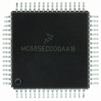
MC68SEC000AA16 Freescale Semiconductor, MC68SEC000AA16 Datasheet - Page 157

MC68SEC000AA16
Manufacturer Part Number
MC68SEC000AA16
Description
IC MPU 32BIT 16MHZ 64-QFP
Manufacturer
Freescale Semiconductor
Series
M68000r
Specifications of MC68SEC000AA16
Processor Type
M680x0 32-Bit
Speed
16MHz
Voltage
3.3V, 5V
Mounting Type
Surface Mount
Package / Case
64-QFP
Processor Series
M680xx
Core
CPU32
Maximum Clock Frequency
16 MHz
Operating Supply Voltage
3.3 V, 5 V
Maximum Operating Temperature
+ 105 C
Mounting Style
SMD/SMT
Minimum Operating Temperature
0 C
Core Size
32 Bit
Cpu Speed
16MHz
Digital Ic Case Style
QFP
No. Of Pins
64
Supply Voltage Range
5V
Operating Temperature Range
0°C To +70°C
Frequency Typ
20MHz
Filter Terminals
SMD
Rohs Compliant
Yes
Clock Frequency
16MHz
Lead Free Status / RoHS Status
Lead free / RoHS Compliant
Features
-
Lead Free Status / Rohs Status
Lead free / RoHS Compliant
Available stocks
Company
Part Number
Manufacturer
Quantity
Price
Company:
Part Number:
MC68SEC000AA16
Manufacturer:
Freescale Semiconductor
Quantity:
10 000
Part Number:
MC68SEC000AA16
Manufacturer:
FREESCALE
Quantity:
20 000
Company:
Part Number:
MC68SEC000AA16R2
Manufacturer:
Freescale Semiconductor
Quantity:
10 000
- Current page: 157 of 242
- Download datasheet (2Mb)
10.10 MC68L11E9/E20 Control Timing
Freescale Semiconductor
Frequency of operation
E-clock period
Crystal frequency
External oscillator frequency
Processor control setup time
Reset input pulse width
Mode programming setup time
Mode programming hold time
Interrupt pulse width, IRQ edge-sensitive mode
Wait recovery startup time
Timer pulse width input capture pulse accumulator input
1. V
2. RESET is recognized during the first clock cycle it is held low. Internal circuitry then drives the pin low for four clock cycles,
t
To guarantee external reset vector
Minimum input time (can be pre-empted by internal reset)
PW
PW
PCSU
otherwise noted
releases the pin, and samples the pin level two cycles later to determine the source of the interrupt. Refer to
Resets and Interrupts
DD
IRQ
TIM
= 3.0 Vdc to 5.5 Vdc, V
Notes
= 1/4 t
= t
= t
1. Rising edge sensitive input
2. Falling edge sensitive input
3. Maximum pulse accumulator clocking rate is E-clock frequency divided by 2.
PA[2:0]
PA[2:0]
CYC
CYC
PA7
PA7
:
CYC
(1) (3)
(2) (3)
+ 20 ns
+ 20 ns
(1)
(2)
+ 75 ns
Characteristic
for further detail.
SS
= 0 Vdc, T
PW
TIM
(1) (2)
M68HC11E Family Data Sheet, Rev. 5.1
A
Figure 10-2. Timer Inputs
= T
L
to T
H
, all timing is shown with respect to 20% V
Symbol
PW
PW
PW
t
f
t
t
PCSU
t
t
XTAL
WRS
4 f
MPS
MPH
CYC
f
RSTL
o
IRQ
TIM
o
1000
1020
1020
Min
325
dc
dc
10
—
—
8
1
2
1.0 MHz
MC68L11E9/E20 Control Timing
Max
1.0
4.0
4.0
—
—
—
—
—
—
—
—
4
DD
Min
500
200
520
520
dc
—
dc
10
—
and 70% V
8
1
2
2.0 MHz
Max
2.0
8.0
8.0
—
—
—
—
—
—
—
—
4
DD
Chapter 5
, unless
MHz
MHz
MHz
Unit
t
t
t
CYC
CYC
CYC
ns
ns
ns
ns
ns
157
Related parts for MC68SEC000AA16
Image
Part Number
Description
Manufacturer
Datasheet
Request
R
Part Number:
Description:
Manufacturer:
Freescale Semiconductor, Inc
Datasheet:
Part Number:
Description:
Manufacturer:
Freescale Semiconductor, Inc
Datasheet:
Part Number:
Description:
Manufacturer:
Freescale Semiconductor, Inc
Datasheet:
Part Number:
Description:
Manufacturer:
Freescale Semiconductor, Inc
Datasheet:
Part Number:
Description:
Manufacturer:
Freescale Semiconductor, Inc
Datasheet:
Part Number:
Description:
Manufacturer:
Freescale Semiconductor, Inc
Datasheet:
Part Number:
Description:
Manufacturer:
Freescale Semiconductor, Inc
Datasheet:
Part Number:
Description:
Manufacturer:
Freescale Semiconductor, Inc
Datasheet:
Part Number:
Description:
Manufacturer:
Freescale Semiconductor, Inc
Datasheet:
Part Number:
Description:
Manufacturer:
Freescale Semiconductor, Inc
Datasheet:
Part Number:
Description:
Manufacturer:
Freescale Semiconductor, Inc
Datasheet:
Part Number:
Description:
Manufacturer:
Freescale Semiconductor, Inc
Datasheet:
Part Number:
Description:
Manufacturer:
Freescale Semiconductor, Inc
Datasheet:
Part Number:
Description:
Manufacturer:
Freescale Semiconductor, Inc
Datasheet:
Part Number:
Description:
Manufacturer:
Freescale Semiconductor, Inc
Datasheet:


