MC68SEC000AA16 Freescale Semiconductor, MC68SEC000AA16 Datasheet - Page 98
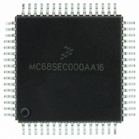
MC68SEC000AA16
Manufacturer Part Number
MC68SEC000AA16
Description
IC MPU 32BIT 16MHZ 64-QFP
Manufacturer
Freescale Semiconductor
Series
M68000r
Specifications of MC68SEC000AA16
Processor Type
M680x0 32-Bit
Speed
16MHz
Voltage
3.3V, 5V
Mounting Type
Surface Mount
Package / Case
64-QFP
Processor Series
M680xx
Core
CPU32
Maximum Clock Frequency
16 MHz
Operating Supply Voltage
3.3 V, 5 V
Maximum Operating Temperature
+ 105 C
Mounting Style
SMD/SMT
Minimum Operating Temperature
0 C
Core Size
32 Bit
Cpu Speed
16MHz
Digital Ic Case Style
QFP
No. Of Pins
64
Supply Voltage Range
5V
Operating Temperature Range
0°C To +70°C
Frequency Typ
20MHz
Filter Terminals
SMD
Rohs Compliant
Yes
Clock Frequency
16MHz
Lead Free Status / RoHS Status
Lead free / RoHS Compliant
Features
-
Lead Free Status / Rohs Status
Lead free / RoHS Compliant
Available stocks
Company
Part Number
Manufacturer
Quantity
Price
Company:

Part Number:
MC68SEC000AA16
Manufacturer:
Freescale Semiconductor
Quantity:
10 000
Part Number:
MC68SEC000AA16
Manufacturer:
FREESCALE
Quantity:
20 000
Company:
Part Number:
MC68SEC000AA16R2
Manufacturer:
Freescale Semiconductor
Quantity:
10 000


6.2 Port A
Port A shares functions with the timer system and has:
DDRA7 — Data Direction for Port A Bit 7
PAEN — Pulse Accumulator System Enable Bit
PAMOD — Pulse Accumulator Mode Bit
PEDGE — Pulse Accumulator Edge Control Bit
DDRA3 — Data Direction for Port A Bit 3
I4/O5 — Input Capture 4/Output Compare 5 Bit
RTR[1:0] — RTI Interrupt Rate Select Bits
98
Parallel Input/Output (I/O) Ports
•
•
•
Overridden if an output compare function is configured to control the PA7 pin
The pulse accumulator uses port A bit 7 as the PAI input, but the pin can also be used as
general-purpose I/O or as an output compare.
Refer to
Refer to
Refer to
This bit is overridden if an output compare function is configured to control the PA3 pin.
Refer to
Refer to
0 = Input
1 = Output
0 = Input
1 = Output
Three input-only pins
Three output-only pins
Two bidirectional I/O pins
Alternate function:
Chapter 9 Timing
Chapter 9 Timing
Chapter 9 Timing
Chapter 9 Timing
Chapter 9 Timing
Even when port A bit 7 is configured as an output, the pin still drives the
input to the pulse accumulator.
Address:
Address:
And/or:
Reset:
Reset:
Read:
Read:
Write:
Write:
Figure 6-2. Pulse Accumulator Control Register (PACTL)
I = Indeterminate after reset
DDRA7
$1000
$1026
OC1
Bit 7
PA7
Bit 7
PAI
0
I
Systems.
Systems.
Systems.
Systems.
Systems.
Figure 6-1. Port A Data Register (PORTA)
PAEWN
M68HC11E Family Data Sheet, Rev. 5.1
OC2
OC1
PA6
6
0
6
0
PAMOD
OC3
OC1
PA5
5
0
5
0
NOTE
PEDGE
OC4
OC1
PA4
4
0
4
0
IC4/OC5
DDRA3
OC1
PA3
3
3
0
I
I4/O5
PA2
IC1
—
2
2
0
I
RTR1
PA1
IC2
—
1
1
0
I
Freescale Semiconductor
RTR0
Bit 0
PA0
Bit 0
IC3
—
0
I
Related parts for MC68SEC000AA16
Image
Part Number
Description
Manufacturer
Datasheet
Request
R

Part Number:
Description:
Manufacturer:
Freescale Semiconductor, Inc
Datasheet:
Part Number:
Description:
Manufacturer:
Freescale Semiconductor, Inc
Datasheet:
Part Number:
Description:
Manufacturer:
Freescale Semiconductor, Inc
Datasheet:
Part Number:
Description:
Manufacturer:
Freescale Semiconductor, Inc
Datasheet:
Part Number:
Description:
Manufacturer:
Freescale Semiconductor, Inc
Datasheet:
Part Number:
Description:
Manufacturer:
Freescale Semiconductor, Inc
Datasheet:
Part Number:
Description:
Manufacturer:
Freescale Semiconductor, Inc
Datasheet:
Part Number:
Description:
Manufacturer:
Freescale Semiconductor, Inc
Datasheet:
Part Number:
Description:
Manufacturer:
Freescale Semiconductor, Inc
Datasheet:
Part Number:
Description:
Manufacturer:
Freescale Semiconductor, Inc
Datasheet:
Part Number:
Description:
Manufacturer:
Freescale Semiconductor, Inc
Datasheet:
Part Number:
Description:
Manufacturer:
Freescale Semiconductor, Inc
Datasheet:
Part Number:
Description:
Manufacturer:
Freescale Semiconductor, Inc
Datasheet:
Part Number:
Description:
Manufacturer:
Freescale Semiconductor, Inc
Datasheet:
Part Number:
Description:
Manufacturer:
Freescale Semiconductor, Inc
Datasheet: