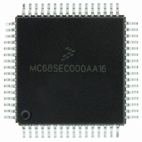
MC68SEC000AA16 Freescale Semiconductor, MC68SEC000AA16 Datasheet - Page 168

MC68SEC000AA16
Manufacturer Part Number
MC68SEC000AA16
Description
IC MPU 32BIT 16MHZ 64-QFP
Manufacturer
Freescale Semiconductor
Series
M68000r
Specifications of MC68SEC000AA16
Processor Type
M680x0 32-Bit
Speed
16MHz
Voltage
3.3V, 5V
Mounting Type
Surface Mount
Package / Case
64-QFP
Processor Series
M680xx
Core
CPU32
Maximum Clock Frequency
16 MHz
Operating Supply Voltage
3.3 V, 5 V
Maximum Operating Temperature
+ 105 C
Mounting Style
SMD/SMT
Minimum Operating Temperature
0 C
Core Size
32 Bit
Cpu Speed
16MHz
Digital Ic Case Style
QFP
No. Of Pins
64
Supply Voltage Range
5V
Operating Temperature Range
0°C To +70°C
Frequency Typ
20MHz
Filter Terminals
SMD
Rohs Compliant
Yes
Clock Frequency
16MHz
Lead Free Status / RoHS Status
Lead free / RoHS Compliant
Features
-
Lead Free Status / Rohs Status
Lead free / RoHS Compliant
Available stocks
Company
Part Number
Manufacturer
Quantity
Price
Company:
Part Number:
MC68SEC000AA16
Manufacturer:
Freescale Semiconductor
Quantity:
10 000
Part Number:
MC68SEC000AA16
Manufacturer:
FREESCALE
Quantity:
20 000
Company:
Part Number:
MC68SEC000AA16R2
Manufacturer:
Freescale Semiconductor
Quantity:
10 000
- Current page: 168 of 242
- Download datasheet (2Mb)
10.15 Expansion Bus Timing Characteristics
168
Electrical Characteristics
Num
1. V
2. Formula only for dc to 2 MHz
3. Input clocks with duty cycles other than 50% affect bus performance. Timing parameters affected by input clock duty cycle
Where:
4a
4b
12
17
18
19
21
22
24
25
26
27
28
29
35
36
1
2
3
9
erwise noted
are identified by (a) and (b). To recalculate the approximate bus timing values, substitute the following expressions in place
of 1/8 t
(a) (1–dc) × 1/4 t
(b) dc × 1/4 t
dc is the decimal value of duty cycle percentage (high time)
DD
Frequency of operation (E-clock frequency)
Cycle time
Pulse width, E low
Pulse width, E high
E and AS rise time
E and AS fall time
Address hold time
Non-multiplexed address valid time to E rise
Read data setup time
Read data hold time, max = t
Write data delay time, t
Write data hold time, t
Multiplexed address valid time to E rise
Multiplexed address valid time to AS fall
Multiplexed address hold time
Delay time, E to AS rise, t
Pulse width, AS high, PW
Delay time, AS to E rise, t
MPU address access time
MPU access time, t
Multiplexed address delay (Previous cycle MPU read)
= 5.0 Vdc ±10%, V
t
t
t
t
t
t
CYC
AV
AVM
ASL
AHL
ACCA
MAD
= PW
in the above formulas, where applicable:
= PW
= 1/8 t
= PW
= t
CYC
= t
ASD
CYC
EL
CYC
ASH
EL
CYC
–(t
+ 30 ns
–(PW
–(t
ASD
–70 ns
–29.5 ns
(2) (3)a
(2)
ASD
(2)
SS
ACCE
Characteristic
, PW
EL
, PW
+ 80 ns)
DHW
= 0 Vdc, T
(2) (3)a
DDW
+ 90 ns)
–t
, t
(2)
AVM
= PW
EL
ASH
ASD
ASED
AH
(2) (3)b
(3)a
EH
= 1/8 t
= 1/8 t
= 1/2 t
MAD
) –t
= 1/8 t
= 1/2 t
(2) (3)a
= 1/4 t
= 1/8 t
EH
= 1/8 t
(2) (3)a
DSR
A
CYC
–t
M68HC11E Family Data Sheet, Rev. 5.1
CYC
CYC
= T
(1)
CYC
DSR
CYC
–t
CYC
CYC
–29.5 ns
CYC
f
L
+ 65.5 ns
–23 ns
–29.5 ns
to T
–28 ns
–9.5 ns
–29 ns
–9.5 ns
H
, all timing is shown with respect to 20% V
(2) (3)a
(2)
(2) (3)a
(2) (3)a
(2) (3)b
Symbol
PW
PW
PW
t
t
t
t
t
t
t
t
t
t
t
ASED
ACCA
ACCE
t
t
DDW
DHW
CYC
t
DSR
DHR
AVM
MAD
t
AHL
ASD
ASL
AH
AV
f
t
t
o
ASH
r
f
EH
EL
281.5
271.5
115.5
115.5
744.5
145.5
1000
95.5
95.5
95.5
Min
477
472
151
221
dc
30
—
—
—
—
0
1.0 MHz
145.5
190.5
Max
442
1.0
—
—
—
20
20
—
—
—
—
—
—
—
—
—
—
—
—
Min Max Min Max
DD
500
227
222
307
dc
33
94
30
33
84
26
33
53
96
53
83
—
—
—
—
2.0 MHz
0
and 70% V
Freescale Semiconductor
128
192
2.0
20
20
83
—
—
—
—
—
—
—
—
—
—
—
—
—
—
—
333
146
141
196
dc
—
—
26
54
30
26
54
13
31
31
63
31
51
3.0 MHz
0
DD
, unless oth-
111
3.0
20
15
51
71
—
—
—
—
—
—
—
—
—
—
—
—
—
—
—
MHz
Unit
ns
ns
ns
ns
ns
ns
ns
ns
ns
ns
ns
ns
ns
ns
ns
ns
ns
ns
ns
ns
Related parts for MC68SEC000AA16
Image
Part Number
Description
Manufacturer
Datasheet
Request
R
Part Number:
Description:
Manufacturer:
Freescale Semiconductor, Inc
Datasheet:
Part Number:
Description:
Manufacturer:
Freescale Semiconductor, Inc
Datasheet:
Part Number:
Description:
Manufacturer:
Freescale Semiconductor, Inc
Datasheet:
Part Number:
Description:
Manufacturer:
Freescale Semiconductor, Inc
Datasheet:
Part Number:
Description:
Manufacturer:
Freescale Semiconductor, Inc
Datasheet:
Part Number:
Description:
Manufacturer:
Freescale Semiconductor, Inc
Datasheet:
Part Number:
Description:
Manufacturer:
Freescale Semiconductor, Inc
Datasheet:
Part Number:
Description:
Manufacturer:
Freescale Semiconductor, Inc
Datasheet:
Part Number:
Description:
Manufacturer:
Freescale Semiconductor, Inc
Datasheet:
Part Number:
Description:
Manufacturer:
Freescale Semiconductor, Inc
Datasheet:
Part Number:
Description:
Manufacturer:
Freescale Semiconductor, Inc
Datasheet:
Part Number:
Description:
Manufacturer:
Freescale Semiconductor, Inc
Datasheet:
Part Number:
Description:
Manufacturer:
Freescale Semiconductor, Inc
Datasheet:
Part Number:
Description:
Manufacturer:
Freescale Semiconductor, Inc
Datasheet:
Part Number:
Description:
Manufacturer:
Freescale Semiconductor, Inc
Datasheet:


