MC68SEC000AA16 Freescale Semiconductor, MC68SEC000AA16 Datasheet - Page 24
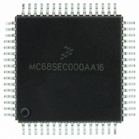
MC68SEC000AA16
Manufacturer Part Number
MC68SEC000AA16
Description
IC MPU 32BIT 16MHZ 64-QFP
Manufacturer
Freescale Semiconductor
Series
M68000r
Specifications of MC68SEC000AA16
Processor Type
M680x0 32-Bit
Speed
16MHz
Voltage
3.3V, 5V
Mounting Type
Surface Mount
Package / Case
64-QFP
Processor Series
M680xx
Core
CPU32
Maximum Clock Frequency
16 MHz
Operating Supply Voltage
3.3 V, 5 V
Maximum Operating Temperature
+ 105 C
Mounting Style
SMD/SMT
Minimum Operating Temperature
0 C
Core Size
32 Bit
Cpu Speed
16MHz
Digital Ic Case Style
QFP
No. Of Pins
64
Supply Voltage Range
5V
Operating Temperature Range
0°C To +70°C
Frequency Typ
20MHz
Filter Terminals
SMD
Rohs Compliant
Yes
Clock Frequency
16MHz
Lead Free Status / RoHS Status
Lead free / RoHS Compliant
Features
-
Lead Free Status / Rohs Status
Lead free / RoHS Compliant
Available stocks
Company
Part Number
Manufacturer
Quantity
Price
Company:

Part Number:
MC68SEC000AA16
Manufacturer:
Freescale Semiconductor
Quantity:
10 000
Part Number:
MC68SEC000AA16
Manufacturer:
FREESCALE
Quantity:
20 000
Company:
Part Number:
MC68SEC000AA16R2
Manufacturer:
Freescale Semiconductor
Quantity:
10 000


General Description
There should be a single pullup resistor near the MCU interrupt input pin (typically 4.7 kΩ). There must
also be an interlock mechanism at each interrupt source so that the source holds the interrupt line low
until the MCU recognizes and acknowledges the interrupt request. If one or more interrupt sources are
still pending after the MCU services a request, the interrupt line will still be held low and the MCU will be
interrupted again as soon as the interrupt mask bit in the MCU is cleared (normally upon return from an
interrupt). Refer to
V
programming. On devices without EPROM/OTPROM, this pin is only an XIRQ input.
1.4.7 MODA and MODB (MODA/LIR and MODB/V
During reset, MODA and MODB select one of the four operating modes:
Refer to
After the operating mode has been selected, the load instruction register (LIR) pin provides an open-drain
output to indicate that execution of an instruction has begun. A series of E-clock cycles occurs during
execution of each instruction. The LIR signal goes low during the first E-clock cycle of each instruction
(opcode fetch). This output is provided for assistance in program debugging.
The V
pin is more than one MOS threshold (about 0.7 volts) above the V
of the reset logic are powered from this signal rather than the V
retained without V
must remain low until V
1.4.8 V
These two inputs provide the reference voltages for the analog-to-digital (A/D) converter circuitry:
For proper A/D converter operation:
24
PPE
•
•
•
•
•
•
•
•
is the input for the 12-volt nominal programming voltage required for EPROM/OTPROM
STBY
Single-chip mode
Expanded mode
Test mode
Bootstrap mode
V
V
V
V
RL
RH
RH
RL
RL
Chapter 2 Operating Modes and On-Chip
is the low reference, typically 0 Vdc.
and V
pin is used to input random-access memory (RAM) standby power. When the voltage on this
is the high reference.
should be at least 3 Vdc greater than V
and V
IRQ must be configured for level-sensitive operation if there is more than
one source of IRQ interrupt.
During EPROM programming of the MC68HC711E9 device, the V
circuitry may latch-up and be damaged if the input current is not limited to
10 mA. For more information please refer to MC68HC711E9 8-Bit
Microcontroller Unit Mask Set Errata 3 (Freescale document order number
68HC711E9MSE3.
RH
DD
RH
Chapter 5 Resets and
should be between V
power applied to the MCU. Reset must be driven low before V
DD
has been restored to a valid level.
M68HC11E Family Data Sheet, Rev. 5.1
SS
Interrupts.
and V
CAUTION
NOTE
DD
RL
Memory.
.
.
STBY
)
DD
DD
input. This allows RAM contents to be
voltage, the internal RAM and part
PPE
Freescale Semiconductor
DD
pin
is removed and
Related parts for MC68SEC000AA16
Image
Part Number
Description
Manufacturer
Datasheet
Request
R

Part Number:
Description:
Manufacturer:
Freescale Semiconductor, Inc
Datasheet:
Part Number:
Description:
Manufacturer:
Freescale Semiconductor, Inc
Datasheet:
Part Number:
Description:
Manufacturer:
Freescale Semiconductor, Inc
Datasheet:
Part Number:
Description:
Manufacturer:
Freescale Semiconductor, Inc
Datasheet:
Part Number:
Description:
Manufacturer:
Freescale Semiconductor, Inc
Datasheet:
Part Number:
Description:
Manufacturer:
Freescale Semiconductor, Inc
Datasheet:
Part Number:
Description:
Manufacturer:
Freescale Semiconductor, Inc
Datasheet:
Part Number:
Description:
Manufacturer:
Freescale Semiconductor, Inc
Datasheet:
Part Number:
Description:
Manufacturer:
Freescale Semiconductor, Inc
Datasheet:
Part Number:
Description:
Manufacturer:
Freescale Semiconductor, Inc
Datasheet:
Part Number:
Description:
Manufacturer:
Freescale Semiconductor, Inc
Datasheet:
Part Number:
Description:
Manufacturer:
Freescale Semiconductor, Inc
Datasheet:
Part Number:
Description:
Manufacturer:
Freescale Semiconductor, Inc
Datasheet:
Part Number:
Description:
Manufacturer:
Freescale Semiconductor, Inc
Datasheet:
Part Number:
Description:
Manufacturer:
Freescale Semiconductor, Inc
Datasheet: