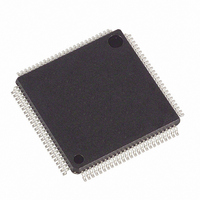
DS21Q58L+ Maxim Integrated Products, DS21Q58L+ Datasheet - Page 12

DS21Q58L+
Manufacturer Part Number
DS21Q58L+
Description
IC TXRX E1 QUAD 3.3V 100LQFP
Manufacturer
Maxim Integrated Products
Datasheet
1.DS21Q58L.pdf
(74 pages)
Specifications of DS21Q58L+
Function
Transceiver
Interface
E1
Number Of Circuits
4
Voltage - Supply
3.14 V ~ 3.47 V
Current - Supply
230mA
Operating Temperature
0°C ~ 70°C
Mounting Type
Surface Mount
Package / Case
100-LQFP
Includes
AIS Alarms Detector and Generator, Loopback Functions, PRBS Generator / Detector, Remote Detector and Generator
Lead Free Status / RoHS Status
Lead free / RoHS Compliant
Power (watts)
-
4.1 Pin Function Descriptions
Table 4-3. System (Backplane) Interface Pins
Table 4-4. Alternate Jitter Attenuator
Table 4-5. Clock Synthesizer
Table 4-6. Parallel Port Control Pins
RD (DS)/SCLK
WR (R/W)/SDI
ALE (AS)/A5
4/8/16MCK
AD7/SDO
AJACKO
SYSCLK
REFCLK
A0 to A4
RSYNC
AJACKI
TSYNC
NAME
NAME
NAME
AD0 to
OUTA
OUTB
NAME
TSER
RSER
TCLK
PBTS
BTS0
BTS1
TS0
TS1
INT
CS
TYPE
TYPE
TYPE
TYPE
I/O
I/O
I/O
I/O
O
O
O
O
O
O
I
I
I
I
I
I
I
I
I
I
I
I
I
I
Transmit Clock. TCLK is a 2.048MHz primary clock that is used to clock data through the transmit
formatter.
Transmit Serial Data. Transmit NRZ serial data. TSER is sampled on the falling edge of TCLK when
IBO is disabled. It is sampled on the falling edge of SYSCLK when the IBO function is enabled.
Receive Sync. An extracted pulse one RCLK wide is output at this pin that identifies either frame or
CAS/CRC4 multiframe boundaries. If the receive elastic store is enabled, this pin can be enabled to be
an input at which a frame-boundary pulse synchronous with SYSCLK is applied.
System Clock. SYSCLK is a 2.048MHz clock used to clock data out of the receive elastic store. When
the IBO is enabled SYSCLK can be a 4.096MHz, 8.192MHz, or 16.384MHz clock.
User-Selectable Output A. OUTA is a multifunction pin the host can program to output various alarms,
clocks, or data, or be used to control external circuitry.
User-Selectable Output B. OUTB is a multifunction pin the host can program to output various alarms,
clocks, or data, or be used to control external circuitry.
Alternate Jitter Attenuator Clock Input. AJACKI is clock input to the alternate jitter attenuator.
Alternate Jitter Attenuator Clock Output. AJACKO is clock output of the alternate jitter attenuator.
4.096MHz/8.192MHz/16.384MHz Clock Output. 4/8/16MCK is a 4.096MHz, 8.192MHz, or 16.384MHz
clock output that is referenced to one of the four recovered line clocks (RCLKs) or to an external
2.048MHz reference.
Reference Clock. REFCLK can be configured as an output to source a 2.048MHz reference clock or as
an input to supply a 2.048MHz reference clock from an external source to the clock synthesizer.
Bus Type Select Bit 0. BTS0 is used with BTS1 to select between muxed, nonmuxed, serial bus
operation, and output high-Z mode.
Transceiver Select Bit 1. TS1 is used with TS0 to select one of four transceivers.
Parallel Bus Type Select. PBTS is used to select between Motorola and Intel parallel bus types.
Data Bus or Address/Data Bus [D0 to D6], Data Bus or Address/Data Bus [D7]/Serial Port Output.
In nonmultiplexed bus operation (MUX = 0), these pins serve as the data bus. In multiplexed bus
operation (MUX = 1), they serve as an 8-bit multiplexed address/data bus.
Address Bus. In nonmultiplexed bus operation, these pins serve as the address bus. In multiplexed bus
operation, these pins are not used and should be wired low.
Chip Select. CS must be low to read or write to the device. It is an active-low signal.
Address Latch Enable (Address Strobe) or A6. In nonmultiplexed bus operation, this pin serves as the
upper address bit. In multiplexed bus operation, it demultiplexes the bus on a positive-going edge.
Write Input (Read/Write)/Serial Port Data Input, Active Low
Transmit Sync. As an input, a pulse at this pin establishes either frame or multiframe boundaries for the
transmitter. As an output, it can be programmed to output either a frame or multiframe pulse.
Receive Serial Data. RSER is the received NRZ serial data. RSER is updated on the rising edges of
RCLK when the receive elastic store is disabled. It is updated on the rising edges of SYSCLK when the
receive elastic store is enabled.
Interrupt. INT flags the host controller during conditions and change of conditions defined in status
registers 1 and 2 and the HDLC status register. It is an active-low, open-drain output.
Bus Type Select Bit 1. BTS1 is used with BTS0 to select between muxed, nonmuxed, serial bus
operation, and output high-Z mode.
Transceiver Select Bit 0. TS0 is used with TS1 to select one of four transceivers.
Read Input—Data Strobe/Serial Port Clock. RD and DS are active-low signals. DS is active high when
in multiplexed mode (Section 26).
12 of 74
FUNCTION
FUNCTION
FUNCTION
FUNCTION


