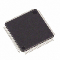
DS21Q58L+ Maxim Integrated Products, DS21Q58L+ Datasheet - Page 13

DS21Q58L+
Manufacturer Part Number
DS21Q58L+
Description
IC TXRX E1 QUAD 3.3V 100LQFP
Manufacturer
Maxim Integrated Products
Datasheet
1.DS21Q58L.pdf
(74 pages)
Specifications of DS21Q58L+
Function
Transceiver
Interface
E1
Number Of Circuits
4
Voltage - Supply
3.14 V ~ 3.47 V
Current - Supply
230mA
Operating Temperature
0°C ~ 70°C
Mounting Type
Surface Mount
Package / Case
100-LQFP
Includes
AIS Alarms Detector and Generator, Loopback Functions, PRBS Generator / Detector, Remote Detector and Generator
Lead Free Status / RoHS Status
Lead free / RoHS Compliant
Power (watts)
-
Table 4-7. Serial Port Control Pins
Table 4-8. Line Interface Pins
Table 4-9. Supply Pins
5. FUNCTIONAL DESCRIPTION
The analog AMI/HDB3 waveform off the E1 line is transformer-coupled into the DS21Q58’s RRING and RTIP pins.
The device recovers clock and data from the analog signal and passes it through the jitter attenuation mux to the
receive framer, where the digital serial stream is analyzed to locate the framing/multiframe pattern. The DS21Q58
contains an active filter that reconstructs the analog-received signal for the nonlinear losses that occur in
transmission. The device has a usable receive sensitivity of 0dB to -12dB. The receive framer locates FAS frame
and CRC and CAS multiframe boundaries as well as detects incoming alarms including carrier loss, loss of
synchronization, AIS, and remote alarm. If needed, the receive elastic store can be enabled to absorb the phase
and frequency differences between the recovered E1 data stream and an asynchronous backplane clock, which is
provided
2.048MHz/4.096MHz/8.192MHz or 16.384MHz clock. The transmit framer is independent of the receive framer in
both the clock requirements and characteristics. The transmit formatter provides the necessary frame/multiframe
data overhead for E1 transmission.
Note: This data sheet assumes a particular nomenclature of the E1 operating environment. In each 125ms frame,
there are 32 8-bit time slots numbered 0 to 31. Time slot 0 is transmitted first and received first. These 32 time slots
are also referred to as channels with a numbering scheme of 1 to 32. Time slot 0 is identical to channel 1, time slot
1 is identical to channel 2, and so on. Each time slot (or channel) is made up of eight bits that are numbered 1 to 8.
Bit number 1, MSB, is transmitted first. Bit number 8, the LSB, is transmitted last. The term “locked” is used to refer
to two clock signals that are phase-locked or frequency-locked or derived from a common clock (i.e., an 8.192MHz
clock can be locked to a 2.048MHz clock if they share the same 8kHz component).
RTIP and
TTIP and
RRING
TRING
NAME
NAME
NAME
OCES
MCLK
DVDD
RVDD
TVDD
DVSS
RVSS
SCLK
TVSS
ICES
SDO
SDI
at
the
Supply
Supply
Supply
Supply
Supply
Supply
TYPE
TYPE
TYPE
O
O
I
I
I
I
I
I
SYSCLK
Serial Port Data Input. Data at this input can be sampled on the rising or falling edge of SCLK.
Serial Port Clock. SCLK is used to clock data into and out of the serial port.
Receive Tip and Ring. RTIP and RRING are analog inputs for clock recovery circuitry. These pins
connect through a 1:1 step-up transformer to the E1 line. See Section
Serial Port Data Output. Data at this output can be updated on the rising or falling edge of SCLK.
Input Clock-Edge Select. ICES is used to select which SCLK clock edge samples data at SDI.
Output Clock-Edge Select. OCES is used to select which SCLK clock edge updates data at SDO.
Master Clock Input. A 2.048MHz (±50ppm) clock source with TTL levels is applied at this pin. This clock
is used internally for both clock/data recovery and for jitter attenuation.
Transmit Tip and Ring. TTIP and TRING are analog line-driver outputs. These pins connect through a
1:2 step-up transformer to the E1 line. See Section
Receive Analog Positive Supply. 3.3V ±5%. Should be wired to the DVDD and TVDD pins.
Digital Positive Supply. 3.3V ±5%. Should be wired to the RVDD and TVDD pins.
Transmit Analog Positive Supply. 3.3V ±5%. Should be wired to the RVDD and DVDD pins.
Digital Signal Ground. 0V. Should be wired to the RVSS and TVSS pins.
Receive Analog Signal Ground. 0V. Should be wired to DVSS and TVSS.
Transmit Analog Signal Ground. 0V. Should be wired to DVSS and RVSS.
input.
The
clock
13 of 74
applied
at
FUNCTION
FUNCTION
FUNCTION
21
the
for details.
SYSCLK
21
input
for details.
can
be
either
a


