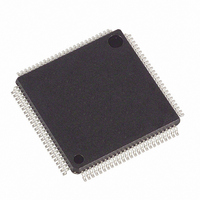
DS21Q58L+ Maxim Integrated Products, DS21Q58L+ Datasheet - Page 45

DS21Q58L+
Manufacturer Part Number
DS21Q58L+
Description
IC TXRX E1 QUAD 3.3V 100LQFP
Manufacturer
Maxim Integrated Products
Datasheet
1.DS21Q58L.pdf
(74 pages)
Specifications of DS21Q58L+
Function
Transceiver
Interface
E1
Number Of Circuits
4
Voltage - Supply
3.14 V ~ 3.47 V
Current - Supply
230mA
Operating Temperature
0°C ~ 70°C
Mounting Type
Surface Mount
Package / Case
100-LQFP
Includes
AIS Alarms Detector and Generator, Loopback Functions, PRBS Generator / Detector, Remote Detector and Generator
Lead Free Status / RoHS Status
Lead free / RoHS Compliant
Power (watts)
-
20.
There are two user-configurable output pins for each transceiver, OUTA and OUTB. These pins can be
programmed to output various clocks, alarms for line monitoring, or logic 0 and 1 levels to control external circuitry.
They can also be used to access transmit data between the framer and transmit LIU. OUTA and OUTB can be
active low or active high when operating as clock and alarm outputs. OUTA is active high if OUTAC.4 = 1 and
active low if OUTAC.3 = 0. OUTB is active high if OUTBC.4 = 1 and active low if OUTBC.4 = 0
mode 0000 to control external circuitry. In this configuration, the OUTA pin follows OUTAC.4 and the OUTB pin
follows OUTBC.4. The OUTAC register also contains a control bit for CMI operation. See Section
about CMI operation.
Register Name:
Register Description:
Register Address:
Bit #
Name
Register Name:
Register Description:
Register Address:
Bit #
Name
NAME
NAME
TTLIE
NRZE
CMIE
CMII
OA4
OA3
OA2
OA1
OA0
OB4
OB3
OB2
OB1
OB0
—
—
USER-CONFIGURABLE OUTPUTS
TTLIE
NRZE
7
7
BIT
BIT
7
6
5
4
3
2
1
0
7
6
5
4
3
2
1
0
CMII
TTL Input Enable. When this bit is set, the receiver can accept TTL
positive and negative data at the RTIP and RRING inputs. The data is
clocked in on the falling edge of MCLK.
CMI Invert. See Section
0 = CMI input data not inverted
1 = CMI input data inverted
CMI Enable. See Section
0 = CMI disabled
1 = CMI enabled
OUTA Control Bit 4. Inverts OUTA output.
OUTA Control Bit 3. See
OUTA Control Bit 2. See
OUTA Control Bit 1. See
OUTA Control Bit 0. See
NRZ Enable. When this bit is set, the receiver can accept TTL-type NRZ
data at the RTIP input. RRING becomes a clock input.
0 = RTIP and RRING are in normal mode.
1 = RTIP becomes an NRZ TTL-type input and RRING is its associated
clock input. Data at RTIP is clocked in on the falling edge of the clock
present on RRING.
Unused. Should be set = 0 for proper operation.
Unused. Should be set = 0 for proper operation.
OUTB Control Bit 4. Inverts OUTB output.
OUTB Control Bit 3
OUTB Control Bit 2
OUTB Control Bit 1
OUTB Control Bit 0
—
6
6
OUTAC
OUTA Control Register
1A Hex
OUTBC
OUTB Control Register
1B Hex
CMIE
—
5
5
OA4
OB4
4
4
22
22
Table 20-1
Table 20-1
Table 20-1
Table 20-1
for details.
for details.
45 of 74
FUNCTION
FUNCTION
OA3
OB3
3
3
for details.
for details.
for details.
for details.
OA2
OB2
2
2
OA1
OB1
1
1
OA0
OB0
0
0
(Table
22
20-1). Select
for details


