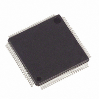
DS21Q58L+ Maxim Integrated Products, DS21Q58L+ Datasheet - Page 51

DS21Q58L+
Manufacturer Part Number
DS21Q58L+
Description
IC TXRX E1 QUAD 3.3V 100LQFP
Manufacturer
Maxim Integrated Products
Datasheet
1.DS21Q58L.pdf
(74 pages)
Specifications of DS21Q58L+
Function
Transceiver
Interface
E1
Number Of Circuits
4
Voltage - Supply
3.14 V ~ 3.47 V
Current - Supply
230mA
Operating Temperature
0°C ~ 70°C
Mounting Type
Surface Mount
Package / Case
100-LQFP
Includes
AIS Alarms Detector and Generator, Loopback Functions, PRBS Generator / Detector, Remote Detector and Generator
Lead Free Status / RoHS Status
Lead free / RoHS Compliant
Power (watts)
-
Figure 21-4. Transmit Waveform Template
21.4 Jitter Attenuators
The DS21Q58 contains an on-board clock and data jitter attenuator for each transceiver and a single, undedicated
“clock only” jitter attenuator. This undedicated jitter attenuator is shown in the block diagram
alternate jitter attenuator.
21.4.1 Clock and Data Jitter Attenuators
The clock and data jitter attenuators can be mapped into the receive or transmit paths and set to buffer depths of
either 32 or 128 bits through the LICR. The 128-bit mode is used in applications where large excursions of wander
are expected. The 32-bit mode is used in delay-sensitive applications. The characteristics of the attenuators are
shown in
appropriately setting or clearing the JAS bit in the LICR. Also, setting the DJA bit in the LICR can disable the jitter
attenuator (in effect, remove it). For the jitter attenuator to operate properly, a 2.048MHz clock (±50ppm) must be
applied at the MCLK pin. On-board circuitry adjusts either the recovered clock from the clock/data recovery block or
the clock applied at the TCLK pin to create a smooth jitter-free clock that is used to clock data out of the jitter
attenuator FIFO. It is acceptable to provide a gapped/bursty clock at the TCLK pin if the jitter attenuator is placed
on the transmit side. If the incoming jitter exceeds either 120UI
is 32 bits), the DS21Q58 divides the internal nominal 32.768MHz clock by either 15 or 17 instead of the normal 16
to keep the buffer from overflowing. When the device divides by either 15 or 17, it also sets the jitter attenuator limit
trip (JALT) bit in the receive information register (RIR.5).
Figure
-0.1
-0.2
21-6. The jitter attenuators can be placed in either the receive path or the transmit path by
1.2
1.1
1.0
0.9
0.8
0.7
0.6
0.5
0.4
0.3
0.2
0.1
0
-250
-200
-150
-100
51 of 74
-50
TIME (ns)
194ns
219ns
0
P-P
(buffer depth is 128 bits) or 28UI
50
100
150
TEMPLATE
269ns
G.703
200
(Figure
250
P-P
(buffer depth
3-1) as the


