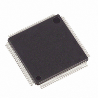
DS21Q58L+ Maxim Integrated Products, DS21Q58L+ Datasheet - Page 36

DS21Q58L+
Manufacturer Part Number
DS21Q58L+
Description
IC TXRX E1 QUAD 3.3V 100LQFP
Manufacturer
Maxim Integrated Products
Datasheet
1.DS21Q58L.pdf
(74 pages)
Specifications of DS21Q58L+
Function
Transceiver
Interface
E1
Number Of Circuits
4
Voltage - Supply
3.14 V ~ 3.47 V
Current - Supply
230mA
Operating Temperature
0°C ~ 70°C
Mounting Type
Surface Mount
Package / Case
100-LQFP
Includes
AIS Alarms Detector and Generator, Loopback Functions, PRBS Generator / Detector, Remote Detector and Generator
Lead Free Status / RoHS Status
Lead free / RoHS Compliant
Power (watts)
-
11.
Registers SA1 and SA16 are used to access the transmit and receive signaling function. Normally, reading these
registers accesses the receive signaling data and writing these registers sources signaling data for the transmitter.
The user can read what was written to the transmit signaling buffer by setting CCR6.5 = 1, then reading
SA1–SA16. In most applications, however, CCR6.5 should be set = 0.
11.1 Receive Signaling
Signaling data is sampled from time slot 16 in the receive data stream and copied into the receive signaling buffers.
The host can access the signaling data by reading SA1 through SA16. The signaling information in these registers
is always updated on multiframe boundaries. The SR2.7 bit in status register 2 can be used to alert the host that
new signaling data is present in the receive signaling buffers. The host has 2ms to read the signaling buffers before
they are updated.
11.2 Transmit Signaling
Insertion of signaling data from the transmit signaling buffers is enabled by setting CCR6.3 = 1. Signaling data is
loaded into the transmit signaling buffers by writing the signaling data to SA1–SA16. On multiframe boundaries, the
contents of the transmit signaling buffer is loaded into a shift register for placement in the appropriate bit position in
the outgoing data stream. The user can use the transmit multiframe interrupt in status register 2 (SR2.5) to know
when to update the signaling bits. The host has 2ms to update the signaling data. The user only needs to update
the signaling data that has changed since the last update.
11.3 CAS Operation
For CAS mode, the user must provide the CAS alignment pattern (four 0s in the upper nibble of TS16). Typically
this is done by setting the upper four bits of SA1 = 0. The lower four bits are alarm bits. The user only needs to
update the appropriate channel associated signaling data in SA2–SA16 on multiframe boundaries.
Register Name:
Register Description:
Register Address:
(MSB)
CH1-A
CH2-A
CH3-A
CH4-A
CH5-A
CH6-A
CH7-A
CH8-A
CH9-A
CH10-A
CH11-A
CH12-A
CH13-A
CH14-A
CH15-A
0
SIGNALING OPERATION
CH1-B
CH2-B
CH3-B
CH4-B
CH5-B
CH6-B
CH7-B
CH8-B
CH9-B
CH10-B
CH11-B
CH12-B
CH13-B
CH14-B
CH15-B
0
CH1-C
CH2-C
CH3-C
CH4-C
CH5-C
CH6-C
CH7-C
CH8-C
CH9-C
CH10-C
CH11-C
CH12-C
CH13-C
CH14-C
CH15-C
SA1 to SA16
Signaling Registers
30h to 3Fh
0
CH1-D
CH2-D
CH3-D
CH4-D
CH5-D
CH6-D
CH7-D
CH8-D
CH9-D
CH10-D
CH11-D
CH12-D
CH13-D
CH14-D
CH15-D
0
CH16-A
CH17-A
CH18-A
CH19-A
CH20-A
CH21-A
CH22-A
CH23-A
CH24-A
CH25-A
CH26-A
CH27-A
CH28-A
CH29-A
CH30-A
X
36 of 74
CH25-B
CH26-B
CH27-B
CH28-B
CH29-B
CH30-B
CH16-B
CH17-B
CH18-B
CH19-B
CH20-B
CH21-B
CH22-B
CH23-B
CH24-B
Y
CH16-C
CH17-C
CH18-C
CH19-C
CH20-C
CH21-C
CH22-C
CH23-C
CH24-C
CH25-C
CH26-C
CH27-C
CH28-C
CH29-C
CH30-C
X
CH16-D
CH17-D
CH18-D
CH19-D
CH20-D
CH21-D
CH22-D
CH23-D
CH24-D
CH25-D
CH26-D
CH27-D
CH28-D
CH29-D
CH30-D
(LSB)
X
SA1
SA2
SA3
SA4
SA5
SA6
SA7
SA8
SA9
SA10
SA11
SA12
SA13
SA14
SA15
SA16


