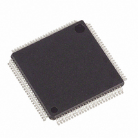
DS21Q58L+ Maxim Integrated Products, DS21Q58L+ Datasheet - Page 40

DS21Q58L+
Manufacturer Part Number
DS21Q58L+
Description
IC TXRX E1 QUAD 3.3V 100LQFP
Manufacturer
Maxim Integrated Products
Datasheet
1.DS21Q58L.pdf
(74 pages)
Specifications of DS21Q58L+
Function
Transceiver
Interface
E1
Number Of Circuits
4
Voltage - Supply
3.14 V ~ 3.47 V
Current - Supply
230mA
Operating Temperature
0°C ~ 70°C
Mounting Type
Surface Mount
Package / Case
100-LQFP
Includes
AIS Alarms Detector and Generator, Loopback Functions, PRBS Generator / Detector, Remote Detector and Generator
Lead Free Status / RoHS Status
Lead free / RoHS Compliant
Power (watts)
-
Table 14-2. System Clock Selection
14.
A single system clock interface (SCI) is common to all four DS21Q58 transceivers. The SCI is designed to allow
any one of the four receivers to act as the master reference clock for the system. When multiple DS21Q58s are
used to build an N port system, the SCI allows any one of the N ports to be the master. The selected reference is
then distributed to the other DS21Q58s through the REFCLK pin. The REFCLK pin acts as an output on the
DS21Q58, which has been selected to provide the reference clock from one of its four receivers. On DS21Q58s not
selected to source the reference clock, this pin becomes an input by writing 0s to the SCSx bits. The reference
clock is also passed to the clock synthesizer PLL to generate a 2.048MHz, 4.096MHz, 8.192MHz, or 16.384MHz
clock. This clock can then be used with the IBO function to merge up to eight E1 lines onto a single high-speed
PCM bus. In the event that the master E1 port fails (enters a receive carrier loss condition), that port automatically
switches to the clock present on the MCLK pin. Therefore, MCLK acts as the backup source of master clock. The
host can then find and select a functioning E1 port as the master. Because the selected port’s clock is passed to
the other DS21Q58s in a multiple device configuration, one DS21Q58’s synthesizer can always be the source of
the high-speed clock. This allows smooth transitions when clock-source switching occurs. The SCI control register
exists in Transceiver 1 only (TS0, TS1 = 0).
Register Name:
Register Description:
Register Address:
Bit #
Name
Table 14-1. Synthesizer Output Select
SCS2
CSS1
AJACKE
0
0
0
0
1
1
1
1
NAME
BUCS
CSS1
CSS0
SCS2
SCS1
SCS0
0
0
1
1
SOE
SYSTEM CLOCK INTERFACE
SCS1
CSS0
0
0
1
1
0
0
1
1
AJACKE
0
1
0
1
7
BIT
SCS0
7
6
5
4
3
2
1
0
0
1
0
1
1
0
1
0
SYNTHESIZER OUTPUT
AJACK Enable. This bit enables the alternate jitter attenuator.
Backup Clock Select. Selects which clock source to switch to
automatically during a loss-of-transmit clock event.
0 = during an LOTC event switch to MCLK
1 = during an LOTC event switch to system reference clock
Synthesizer Output Enable
0 = 2/4/8/16MCK pin in high-Z mode
1 = 2/4/8/16MCK pin active
Clock Synthesizer Select Bit 1
Clock Synthesizer Select Bit 0
System Clock Select Bit 2
System Clock Select Bit 1
System Clock Select Bit 0
BUCS
FREQUENCY (MHz)
None (Master Port can be derived from another DS21Q58 in the system.)
SCICR
System Clock Interface Control Register
(Note: This register is valid only for Transceiver 1 (TS0 = 0, TS1 = 0).)
1D Hex
6
16.384
2.048
4.096
8.192
SOE
5
PORT SELECTED AS MASTER
CSS1
Reserved for future use.
Reserved for future use.
Reserved for future use.
4
(Table
(Table
(Table
Transceiver 1
Transceiver 2
Transceiver 3
Transceiver 4
40 of 74
FUNCTION
(Table
(Table
CSS0
14-2)
14-2)
14-2)
3
14-1)
14-1)
SCS2
2
SCS1
1
DS21Q58 E1 Quad Transceiver
SCS0
0


