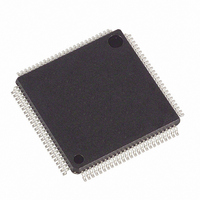
DS21Q58L+ Maxim Integrated Products, DS21Q58L+ Datasheet - Page 17

DS21Q58L+
Manufacturer Part Number
DS21Q58L+
Description
IC TXRX E1 QUAD 3.3V 100LQFP
Manufacturer
Maxim Integrated Products
Datasheet
1.DS21Q58L.pdf
(74 pages)
Specifications of DS21Q58L+
Function
Transceiver
Interface
E1
Number Of Circuits
4
Voltage - Supply
3.14 V ~ 3.47 V
Current - Supply
230mA
Operating Temperature
0°C ~ 70°C
Mounting Type
Surface Mount
Package / Case
100-LQFP
Includes
AIS Alarms Detector and Generator, Loopback Functions, PRBS Generator / Detector, Remote Detector and Generator
Lead Free Status / RoHS Status
Lead free / RoHS Compliant
Power (watts)
-
Note 1: The device ID register and the system clock-interface control register exist in Transceiver 1 only (TS0, TS1 = 0).
Note 2: Only the factory uses the test register; this register must be cleared (set to all zeros) on power-up initialization to ensure proper
8. CONTROL, ID, AND TEST REGISTERS
The DS21Q58 operation is configured through a set of nine control registers. Typically, the control registers are
only accessed when the system is first powered up. Once the device has been initialized, the control registers only
need to be accessed when there is a change in the system configuration. There is one receive control register
(RCR), one transmit control register (TCR), and seven common control registers (CCR1 to CCR7). Each of these
registers is described in this section.
Address 0Fh has a device identification register (IDR). The four MSBs of this read-only register are fixed to 1 0 0 1,
indicating that a DS21Q58 E1 quad transceiver is present. The lower 4 bits of the IDR are used to identify the
revision of the device. This register exists in Transceiver 1 only (TS0, TS1 = 0).
The factory in testing the DS21Q58 uses the test register at addresses 1E. On power-up, the test register should
be set to 00h for the DS21Q58 to properly operate.
Register Name:
Register Description:
Register Address:
Bit #
Name
NAME
ADDRESS
ID3
ID2
ID1
ID0
1
0
1
0
3C
3D
37
38
39
3A
3B
3E
3F
operation.
7
1
BIT
7
6
5
4
3
1
2
0
TYPE
R/W
R/W
R/W
R/W
R/W
R/W
R/W
R/W
R/W
Bit 7
Bit 6
Bit 5
Bit 4
Chip Revision Bit 3. MSB of a decimal code that represents the chip revision.
Chip Revision Bit 2
Chip Revision Bit 1
Chip Revision Bit 0. LSB of a decimal code that represents the chip revision.
6
0
IDR
Device Identification Register
0F Hex
NAME
SA10
SA11
SA12
SA13
SA14
SA15
SA16
SA8
SA9
5
1
Signaling Access Register 8
Signaling Access Register 9
Signaling Access Register 10
Signaling Access Register 11
Signaling Access Register 12
Signaling Access Register 13
Signaling Access Register 14
Signaling Access Register 15
Signaling Access Register 16
0
4
17 of 74
FUNCTION
ID3
3
FUNCTION
ID2
2
ID1
1
ID0
0


