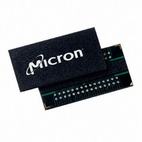
MT41J64M16LA-187E:B TR Micron Technology Inc, MT41J64M16LA-187E:B TR Datasheet - Page 119

MT41J64M16LA-187E:B TR
Manufacturer Part Number
MT41J64M16LA-187E:B TR
Description
IC DDR3 SDRAM 1GBIT 96FBGA
Manufacturer
Micron Technology Inc
Type
DDR3 SDRAMr
Specifications of MT41J64M16LA-187E:B TR
Format - Memory
RAM
Memory Type
DDR3 SDRAM
Memory Size
1G (64M x 16)
Speed
533MHz
Interface
Parallel
Voltage - Supply
1.425 V ~ 1.575 V
Operating Temperature
0°C ~ 95°C
Package / Case
96-FBGA
Organization
64Mx16
Density
1Gb
Address Bus
16b
Maximum Clock Rate
1.066GHz
Operating Supply Voltage (typ)
1.5V
Package Type
FBGA
Operating Temp Range
0C to 95C
Operating Supply Voltage (max)
1.575V
Operating Supply Voltage (min)
1.425V
Supply Current
265mA
Pin Count
96
Mounting
Surface Mount
Operating Temperature Classification
Commercial
Lead Free Status / RoHS Status
Lead free / RoHS Compliant
Other names
557-1378-2
- Current page: 119 of 208
- Download datasheet (13Mb)
Figure 44: DLL Disable Mode to DLL Enable Mode
PDF: 09005aef826aa906
1Gb_DDR3_SDRAM.pdf – Rev. J 05/10 EN
Command
ODT 10
CK#
CKE
CK
ODTL off + 1 × t CK
7
NOP
T0
Notes:
SRE 1
Ta0
The clock frequency range for the DLL disable mode is specified by the parameter
t
supported.
DLL disable mode will affect the read data clock to data strobe relationship (
but not the data strobe to data relationship (
line up read data to the controller time domain.
Compared to the DLL on mode where
cycles after the READ command, the DLL disable mode
after the READ command.
WRITE operations function similarly between the DLL enable and DLL disable modes;
however, ODT functionality is not allowed with DLL disable mode.
CKdll_dis. Due to latency counter and timing restrictions, only CL = 6 and CWL = 6 are
10. Static LOW in the case that R
1. Enter SELF REFRESH.
2. Exit SELF REFRESH.
3. Wait
4. Wait
5. Wait
6. Wait
7. Starting with the idle state.
8. Change frequency.
9. Clock must be stable at least
t CKSRE
NOP
Ta1
t
t
t
t
XS, then set MR1[0] to 0 to enable DLL.
MRD, then set MR0[8] to 1 to begin DLL RESET.
MRD, update registers (CL, CWL, and write recovery may be necessary).
MOD, any valid command.
Tb0
t CKESR
8
Tc0
119
TT,nom
t
t CKSRX 9
CKSRX.
Tc1
or R
t
DQSCK starts from the rising clock edge AL + CL
Micron Technology, Inc. reserves the right to change products or specifications without notice.
TT(WR)
SRX 2
Td0
t
DQSQ,
1Gb: x4, x8, x16 DDR3 SDRAM
is enabled; otherwise, static LOW or HIGH.
t XS
MRS 3
Te0
t
QH). Special attention is needed to
t MRD
t
Indicates A Break in
Time Scale
DQSCK starts AL + CL - 1 cycles
MRS 4
Tf0
© 2006 Micron Technology, Inc. All rights reserved.
t MRD
t DLLK
MRS 5
Tg0
Commands
t
Don’t Care
DQSCK)
Valid 6
Valid
Th0
Related parts for MT41J64M16LA-187E:B TR
Image
Part Number
Description
Manufacturer
Datasheet
Request
R

Part Number:
Description:
IC DDR3 SDRAM 1GBIT 96FBGA
Manufacturer:
Micron Technology Inc
Datasheet:

Part Number:
Description:
Manufacturer:
Micron Technology Inc
Datasheet:

Part Number:
Description:
Manufacturer:
Micron Technology Inc
Datasheet:

Part Number:
Description:
Manufacturer:
Micron Technology Inc
Datasheet:

Part Number:
Description:
IC SDRAM 64MBIT 133MHZ 54TSOP
Manufacturer:
Micron Technology Inc
Datasheet:

Part Number:
Description:
IC SDRAM 64MBIT 5.5NS 86TSOP
Manufacturer:
Micron Technology Inc
Datasheet:

Part Number:
Description:
IC SDRAM 64MBIT 200MHZ 86TSOP
Manufacturer:
Micron Technology Inc
Datasheet:

Part Number:
Description:
IC SDRAM 64MBIT 133MHZ 54TSOP
Manufacturer:
Micron Technology Inc
Datasheet:

Part Number:
Description:
IC SDRAM 128MBIT 133MHZ 54TSOP
Manufacturer:
Micron Technology Inc
Datasheet:

Part Number:
Description:
IC SDRAM 256MBIT 133MHZ 90VFBGA
Manufacturer:
Micron Technology Inc
Datasheet:

Part Number:
Description:
IC SDRAM 128MBIT 133MHZ 54TSOP
Manufacturer:
Micron Technology Inc
Datasheet:

Part Number:
Description:
IC SDRAM 256MBIT 133MHZ 54TSOP
Manufacturer:
Micron Technology Inc
Datasheet:

Part Number:
Description:
IC DDR SDRAM 512MBIT 6NS 66TSOP
Manufacturer:
Micron Technology Inc
Datasheet:

Part Number:
Description:
IC SDRAM 128MBIT 167MHZ 86TSOP
Manufacturer:
Micron Technology Inc
Datasheet:

Part Number:
Description:
IC SDRAM 128MBIT 143MHZ 86TSOP
Manufacturer:
Micron Technology Inc
Datasheet:


