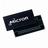
MT41J64M16LA-187E:B TR Micron Technology Inc, MT41J64M16LA-187E:B TR Datasheet - Page 149

MT41J64M16LA-187E:B TR
Manufacturer Part Number
MT41J64M16LA-187E:B TR
Description
IC DDR3 SDRAM 1GBIT 96FBGA
Manufacturer
Micron Technology Inc
Type
DDR3 SDRAMr
Specifications of MT41J64M16LA-187E:B TR
Format - Memory
RAM
Memory Type
DDR3 SDRAM
Memory Size
1G (64M x 16)
Speed
533MHz
Interface
Parallel
Voltage - Supply
1.425 V ~ 1.575 V
Operating Temperature
0°C ~ 95°C
Package / Case
96-FBGA
Organization
64Mx16
Density
1Gb
Address Bus
16b
Maximum Clock Rate
1.066GHz
Operating Supply Voltage (typ)
1.5V
Package Type
FBGA
Operating Temp Range
0C to 95C
Operating Supply Voltage (max)
1.575V
Operating Supply Voltage (min)
1.425V
Supply Current
265mA
Pin Count
96
Mounting
Surface Mount
Operating Temperature Classification
Commercial
Lead Free Status / RoHS Status
Lead free / RoHS Compliant
Other names
557-1378-2
- Current page: 149 of 208
- Download datasheet (13Mb)
MPR Read Predefined Pattern
MODE REGISTER SET (MRS) Command
PDF: 09005aef826aa906
1Gb_DDR3_SDRAM.pdf – Rev. J 05/10 EN
The predetermined read calibration pattern is a fixed pattern of 0, 1, 0, 1, 0, 1, 0, 1. The
following is an example of using the read out predetermined read calibration pattern.
The example is to perform multiple reads from the multipurpose register to do system
level read timing calibration based on the predetermined and standardized pattern.
The following protocol outlines the steps used to perform the read calibration:
The mode registers are loaded via inputs BA[2:0], A[13:0]. BA[2:0] determine which
mode register is programmed:
• BA2 = 0, BA1 = 0, BA0 = 0 for MR0
• BA2 = 0, BA1 = 0, BA0 = 1 for MR1
• BA2 = 0, BA1 = 1, BA0 = 0 for MR2
• BA2 = 0, BA1 = 1, BA0 = 1 for MR3
The MRS command can only be issued (or reissued) when all banks are idle and in the
precharged state (
must wait the specified time
ACTIVATE command (see Figure 51 (page 130)). There is also a restriction after issuing
an MRS command with regard to when the updated functions become available. This
parameter is specified by
ure 51 (page 130) and Figure 52 (page 131). Violating either of these requirements will
result in unspecified operation.
1. Precharge all banks
2. After
3. Data WRITE operations are not allowed until the MPR returns to the normal
4. Issue a read with burst order information (all other address pins are “Don’t Care”):
5. After RL = AL + CL, the DRAM bursts out the predefined read calibration pattern
6. The memory controller repeats the calibration reads until read data capture at
7. After the last MPR READ burst and after
8. When
sequent reads and loads the predefined pattern into the MPR. As soon as
and
DRAM state
• A[1:0] = 00 (data burst order is fixed starting at nibble)
• A2 = 0 (for BL8, burst order is fixed as 0, 1, 2, 3, 4, 5, 6, 7)
• A12 = 1 (use BL8)
(0, 1, 0, 1, 0, 1, 0, 1)
memory controller is optimized
MR3[2] = 0, and MR3[1:0] = “Don’t Care” to the normal DRAM state. All subse-
quent read and write accesses will be regular reads and writes from/to the DRAM
array
mands (such as activate a memory bank for regular read or write access) are
permitted
t
MOD are satisfied, the MPR is available
t
RP is satisfied, set MRS, MR3[2] = 1 and MR3[1:0] = 00. This redirects all sub-
t
MRD and
t
RP is satisfied and no data bursts are in progress). The controller
t
MOD are satisfied from the last MRS, the regular DRAM com-
t
MOD. Both
t
149
MRD before initiating a subsequent operation such as an
MODE REGISTER SET (MRS) Command
t
MRD and
Micron Technology, Inc. reserves the right to change products or specifications without notice.
t
MPRR has been satisfied, issue MRS,
1Gb: x4, x8, x16 DDR3 SDRAM
t
MOD parameters are shown in Fig-
© 2006 Micron Technology, Inc. All rights reserved.
t
MRD
Related parts for MT41J64M16LA-187E:B TR
Image
Part Number
Description
Manufacturer
Datasheet
Request
R

Part Number:
Description:
IC DDR3 SDRAM 1GBIT 96FBGA
Manufacturer:
Micron Technology Inc
Datasheet:

Part Number:
Description:
Manufacturer:
Micron Technology Inc
Datasheet:

Part Number:
Description:
Manufacturer:
Micron Technology Inc
Datasheet:

Part Number:
Description:
Manufacturer:
Micron Technology Inc
Datasheet:

Part Number:
Description:
IC SDRAM 64MBIT 133MHZ 54TSOP
Manufacturer:
Micron Technology Inc
Datasheet:

Part Number:
Description:
IC SDRAM 64MBIT 5.5NS 86TSOP
Manufacturer:
Micron Technology Inc
Datasheet:

Part Number:
Description:
IC SDRAM 64MBIT 200MHZ 86TSOP
Manufacturer:
Micron Technology Inc
Datasheet:

Part Number:
Description:
IC SDRAM 64MBIT 133MHZ 54TSOP
Manufacturer:
Micron Technology Inc
Datasheet:

Part Number:
Description:
IC SDRAM 128MBIT 133MHZ 54TSOP
Manufacturer:
Micron Technology Inc
Datasheet:

Part Number:
Description:
IC SDRAM 256MBIT 133MHZ 90VFBGA
Manufacturer:
Micron Technology Inc
Datasheet:

Part Number:
Description:
IC SDRAM 128MBIT 133MHZ 54TSOP
Manufacturer:
Micron Technology Inc
Datasheet:

Part Number:
Description:
IC SDRAM 256MBIT 133MHZ 54TSOP
Manufacturer:
Micron Technology Inc
Datasheet:

Part Number:
Description:
IC DDR SDRAM 512MBIT 6NS 66TSOP
Manufacturer:
Micron Technology Inc
Datasheet:

Part Number:
Description:
IC SDRAM 128MBIT 167MHZ 86TSOP
Manufacturer:
Micron Technology Inc
Datasheet:

Part Number:
Description:
IC SDRAM 128MBIT 143MHZ 86TSOP
Manufacturer:
Micron Technology Inc
Datasheet:


