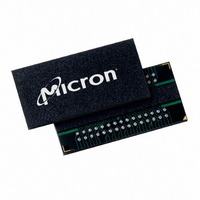
MT41J64M16LA-187E:B TR Micron Technology Inc, MT41J64M16LA-187E:B TR Datasheet - Page 65

MT41J64M16LA-187E:B TR
Manufacturer Part Number
MT41J64M16LA-187E:B TR
Description
IC DDR3 SDRAM 1GBIT 96FBGA
Manufacturer
Micron Technology Inc
Type
DDR3 SDRAMr
Specifications of MT41J64M16LA-187E:B TR
Format - Memory
RAM
Memory Type
DDR3 SDRAM
Memory Size
1G (64M x 16)
Speed
533MHz
Interface
Parallel
Voltage - Supply
1.425 V ~ 1.575 V
Operating Temperature
0°C ~ 95°C
Package / Case
96-FBGA
Organization
64Mx16
Density
1Gb
Address Bus
16b
Maximum Clock Rate
1.066GHz
Operating Supply Voltage (typ)
1.5V
Package Type
FBGA
Operating Temp Range
0C to 95C
Operating Supply Voltage (max)
1.575V
Operating Supply Voltage (min)
1.425V
Supply Current
265mA
Pin Count
96
Mounting
Surface Mount
Operating Temperature Classification
Commercial
Lead Free Status / RoHS Status
Lead free / RoHS Compliant
Other names
557-1378-2
- Current page: 65 of 208
- Download datasheet (13Mb)
Alternative 40 Ohm Driver
Table 43: 40 Ohm Driver Impedance Characteristics
40 Ohm Output Driver Sensitivity
Table 44: 40 Ohm Output Driver Sensitivity Definition
PDF: 09005aef826aa906
1Gb_DDR3_SDRAM.pdf – Rev. J 05/10 EN
R
R
R
R
R
R
MR1[5,1]
ON(PD)
ON(PD)
ON(PD)
ON(PU)
ON(PU)
ON(PU)
Pull-up/pull-down mismatch (MM
0,0
Symbol
@ 0.2 × V
@ 0.5 × V
@ 0.8 × V
@ 0.2 × V
@ 0.5 × V
@ 0.8 × V
DDQ
DDQ
DDQ
DDQ
DDQ
DDQ
R
40Ω
ON
Notes:
Note:
0.9 - dR
0.9 - dR
0.9 - dR
0.6 - dR
0.6 - dR
0.9 - dR
If either the temperature or the voltage changes after I/O calibration, then the tolerance
limits listed in Table 43 can be expected to widen according to Table 44 and Table 45
(page 66).
1. Tolerance limits assume RZQ of 240Ω (±1%) and are applicable after proper ZQ calibra-
2. Measurement definition for mismatch between pull-up and pull-down (MM
3. For IT and AT (1Gb only) devices, the minimum values are derated by 6% when the de-
1. ΔT = T - T(@ calibration), ΔV = V
Resistor
R
R
ON
ON
ON
ON
tion has been performed at a stable temperature and voltage (V
Refer to 40 Ohm Output Driver Sensitivity (page 65) if either the temperature or the
voltage changes after calibration.
ure both R
MM
vice operates between –40°C and 0°C (T
ON
ON
ON40(PD)
ON40(PU)
dTM × |ΔT| - dR
dTM × |ΔT| - dR
dTH × |ΔT| - dR
dTH × |ΔT| - dR
dTL × |ΔT| - dR
dTL × |ΔT| - dR
PUPD
PUPD
)
=
Min
Ron
ON(PU)
Ron
PU
- Ron
and R
ON
ON
ON
ON
ON
ON
NOM
0.2 × V
0.5 × V
0.8 × V
0.2 × V
0.5 × V
0.8 × V
0.5 × V
dVL × |ΔV|
dVM × |ΔV|
dVH × |ΔV|
dVL × |ΔV|
dVM × |ΔV|
dVH × |ΔV|
V
PD
OUT
ON(PD)
× 100
DDQ
DDQ
DDQ
DDQ
DDQ
DDQ
DDQ
65
at 0.5 × V
DDQ
1.1 + dR
1.1 + dR
- V
Micron Technology, Inc. reserves the right to change products or specifications without notice.
1.4 + dR
1.1 + dR
–10%
1.1 + dR
1.4 + dR
Min
0.6
0.9
0.9
0.9
0.9
0.6
DDQ
DDQ
C
).
:
(@ calibration), and V
ON
ON
ON
ON
1Gb: x4, x8, x16 DDR3 SDRAM
ON
ON
dTM × |ΔT| + dR
dTM × |ΔT| + dR
dTH × |ΔT| + dR
dTH × |ΔT| + dR
dTL × |ΔT| + dR
dTL × |ΔT| + dR
Output Driver Impedance
Nom
1.0
1.0
1.0
1.0
1.0
1.0
n/a
Max
© 2006 Micron Technology, Inc. All rights reserved.
ON
ON
ON
ON
ON
ON
DD
DDQ
dVL × |ΔV|
dVM × |ΔV|
dVH × |ΔV|
dVL × |ΔV|
dVM × |ΔV|
dVH × |ΔV|
Max
1.1
1.1
1.4
1.4
1.1
1.1
= V
10
= V
DDQ
DD
.
, V
PUPD
SSQ
RZQ/6
RZQ/6
RZQ/6
RZQ/6
RZQ/6
RZQ/6
Units
). Meas-
= V
RZQ/6
RZQ/6
RZQ/6
RZQ/6
RZQ/6
RZQ/6
Units
%
SS
).
Related parts for MT41J64M16LA-187E:B TR
Image
Part Number
Description
Manufacturer
Datasheet
Request
R

Part Number:
Description:
IC DDR3 SDRAM 1GBIT 96FBGA
Manufacturer:
Micron Technology Inc
Datasheet:

Part Number:
Description:
Manufacturer:
Micron Technology Inc
Datasheet:

Part Number:
Description:
Manufacturer:
Micron Technology Inc
Datasheet:

Part Number:
Description:
Manufacturer:
Micron Technology Inc
Datasheet:

Part Number:
Description:
IC SDRAM 64MBIT 133MHZ 54TSOP
Manufacturer:
Micron Technology Inc
Datasheet:

Part Number:
Description:
IC SDRAM 64MBIT 5.5NS 86TSOP
Manufacturer:
Micron Technology Inc
Datasheet:

Part Number:
Description:
IC SDRAM 64MBIT 200MHZ 86TSOP
Manufacturer:
Micron Technology Inc
Datasheet:

Part Number:
Description:
IC SDRAM 64MBIT 133MHZ 54TSOP
Manufacturer:
Micron Technology Inc
Datasheet:

Part Number:
Description:
IC SDRAM 128MBIT 133MHZ 54TSOP
Manufacturer:
Micron Technology Inc
Datasheet:

Part Number:
Description:
IC SDRAM 256MBIT 133MHZ 90VFBGA
Manufacturer:
Micron Technology Inc
Datasheet:

Part Number:
Description:
IC SDRAM 128MBIT 133MHZ 54TSOP
Manufacturer:
Micron Technology Inc
Datasheet:

Part Number:
Description:
IC SDRAM 256MBIT 133MHZ 54TSOP
Manufacturer:
Micron Technology Inc
Datasheet:

Part Number:
Description:
IC DDR SDRAM 512MBIT 6NS 66TSOP
Manufacturer:
Micron Technology Inc
Datasheet:

Part Number:
Description:
IC SDRAM 128MBIT 167MHZ 86TSOP
Manufacturer:
Micron Technology Inc
Datasheet:

Part Number:
Description:
IC SDRAM 128MBIT 143MHZ 86TSOP
Manufacturer:
Micron Technology Inc
Datasheet:


