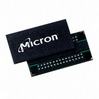
MT41J64M16LA-187E:B TR Micron Technology Inc, MT41J64M16LA-187E:B TR Datasheet - Page 135

MT41J64M16LA-187E:B TR
Manufacturer Part Number
MT41J64M16LA-187E:B TR
Description
IC DDR3 SDRAM 1GBIT 96FBGA
Manufacturer
Micron Technology Inc
Type
DDR3 SDRAMr
Specifications of MT41J64M16LA-187E:B TR
Format - Memory
RAM
Memory Type
DDR3 SDRAM
Memory Size
1G (64M x 16)
Speed
533MHz
Interface
Parallel
Voltage - Supply
1.425 V ~ 1.575 V
Operating Temperature
0°C ~ 95°C
Package / Case
96-FBGA
Organization
64Mx16
Density
1Gb
Address Bus
16b
Maximum Clock Rate
1.066GHz
Operating Supply Voltage (typ)
1.5V
Package Type
FBGA
Operating Temp Range
0C to 95C
Operating Supply Voltage (max)
1.575V
Operating Supply Voltage (min)
1.425V
Supply Current
265mA
Pin Count
96
Mounting
Surface Mount
Operating Temperature Classification
Commercial
Lead Free Status / RoHS Status
Lead free / RoHS Compliant
Other names
557-1378-2
- Current page: 135 of 208
- Download datasheet (13Mb)
Mode Register 1 (MR1)
Figure 55: Mode Register 1 (MR1) Definition
DLL Enable/DLL Disable
PDF: 09005aef826aa906
1Gb_DDR3_SDRAM.pdf – Rev. J 05/10 EN
M15
0
0
1
1
M14
0
1
0
1
Mode register set 0 (MR0)
Mode register set 1 (MR1)
Mode register set 2 (MR2)
Mode register set 3 (MR3)
Mode Register
Notes:
The mode register 1 (MR1) controls additional functions and features not available in
the other mode registers: Q OFF (OUTPUT DISABLE), TDQS (for the x8 configuration
only), DLL ENABLE/DLL DISABLE, R
CAS ADDITIVE latency, and OUTPUT DRIVE STRENGTH. These functions are control-
led via the bits shown in Figure 55 (page 135). The MR1 register is programmed via the
MRS command and retains the stored information until it is reprogrammed, until RE-
SET# goes LOW, or until the device loses power. Reprogramming the MR1 register will
not alter the contents of the memory array, provided it is performed correctly.
The MR1 register must be loaded when all banks are idle and no bursts are in progress.
The controller must satisfy the specified timing parameters
tiating a subsequent operation.
The DLL may be enabled or disabled by programming MR1[0] during the LOAD MODE
command, as shown in Figure 55 (page 135). The DLL must be enabled for normal oper-
ation. DLL enable is required during power-up initialization and upon returning to
normal operation after having disabled the DLL for the purpose of debugging or evalua-
tion. Enabling the DLL should always be followed by resetting the DLL using the
appropriate LOAD MODE command.
1. MR1[16, 13, 10, 8] are reserved for future use and must be programmed to 0.
2. During write leveling, if MR1[7] and MR1[12] are 1, then all R
3. During write leveling, if MR1[7] is a 1, but MR1[12] is a 0, then only R
for use.
are available for use.
M9
0
0
0
0
1
1
1
1
0 1
M6
16
BA2
0
0
1
1
0
0
1
1
M12
0
1
M2
0
1
0
1
0
1
0
1
0
BA1
15
Disabled
Enabled
RZQ/2 (120Ω [NOM])
RZQ/12 (20Ω [NOM])
RZQ/4 (60Ω [NOM])
RZQ/6 (40Ω [NOM])
RZQ/8 (30Ω [NOM])
Q Off
14
1
BA0
R
R
TT,nom
TT,nom
Non-Writes
0 1
Reserved
Reserved
13
A13
Q Off
disabled
M11
(ODT) 2
12
A12 A11
0
1
TDQS
11
Disabled
Enabled
TDQS
0 1
10
A10
RZQ/2 (120Ω [NOM])
RZQ/4 (60Ω [NOM])
RZQ/6 (40Ω [NOM])
135
R
R
R
TT,nom
TT
TT,nom
9
A9
Reserved
Reserved
Writes
0 1
n/a
n/a
8
A8
disabled
(ODT) 3
WL
7
A7 A6 A5 A4 A3
TT,nom
R
TT
6
Micron Technology, Inc. reserves the right to change products or specifications without notice.
ODS
5
M4
M7
0
0
1
1
0
1
4
value (ODT), WRITE LEVELING, POSTED
M3
AL
Write Levelization
0
1
0
1
Disable (normal)
3
Additive Latency (AL)
1Gb: x4, x8, x16 DDR3 SDRAM
Enable
R
Disabled (AL = 0)
TT
2
A2 A1 A0
AL = CL - 1
AL = CL - 2
ODS DLL
Reserved
1
0
Mode Register 1 (MR1)
M5
Address bus
Mode register 1 (MR1)
0
0
1
1
t
MRD and
M0
M1
0
1
0
1
0
1
© 2006 Micron Technology, Inc. All rights reserved.
TT,nom
Output Drive Strength
RZQ/6 (40Ω [NOM])
RZQ/7 (34Ω [NOM])
Enable (normal)
DLL Enable
Disable
Reserved
Reserved
values are available
TT,nom
t
MOD before ini-
write values
Related parts for MT41J64M16LA-187E:B TR
Image
Part Number
Description
Manufacturer
Datasheet
Request
R

Part Number:
Description:
IC DDR3 SDRAM 1GBIT 96FBGA
Manufacturer:
Micron Technology Inc
Datasheet:

Part Number:
Description:
Manufacturer:
Micron Technology Inc
Datasheet:

Part Number:
Description:
Manufacturer:
Micron Technology Inc
Datasheet:

Part Number:
Description:
Manufacturer:
Micron Technology Inc
Datasheet:

Part Number:
Description:
IC SDRAM 64MBIT 133MHZ 54TSOP
Manufacturer:
Micron Technology Inc
Datasheet:

Part Number:
Description:
IC SDRAM 64MBIT 5.5NS 86TSOP
Manufacturer:
Micron Technology Inc
Datasheet:

Part Number:
Description:
IC SDRAM 64MBIT 200MHZ 86TSOP
Manufacturer:
Micron Technology Inc
Datasheet:

Part Number:
Description:
IC SDRAM 64MBIT 133MHZ 54TSOP
Manufacturer:
Micron Technology Inc
Datasheet:

Part Number:
Description:
IC SDRAM 128MBIT 133MHZ 54TSOP
Manufacturer:
Micron Technology Inc
Datasheet:

Part Number:
Description:
IC SDRAM 256MBIT 133MHZ 90VFBGA
Manufacturer:
Micron Technology Inc
Datasheet:

Part Number:
Description:
IC SDRAM 128MBIT 133MHZ 54TSOP
Manufacturer:
Micron Technology Inc
Datasheet:

Part Number:
Description:
IC SDRAM 256MBIT 133MHZ 54TSOP
Manufacturer:
Micron Technology Inc
Datasheet:

Part Number:
Description:
IC DDR SDRAM 512MBIT 6NS 66TSOP
Manufacturer:
Micron Technology Inc
Datasheet:

Part Number:
Description:
IC SDRAM 128MBIT 167MHZ 86TSOP
Manufacturer:
Micron Technology Inc
Datasheet:

Part Number:
Description:
IC SDRAM 128MBIT 143MHZ 86TSOP
Manufacturer:
Micron Technology Inc
Datasheet:


