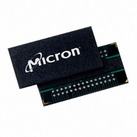
MT41J64M16LA-187E:B TR Micron Technology Inc, MT41J64M16LA-187E:B TR Datasheet - Page 84

MT41J64M16LA-187E:B TR
Manufacturer Part Number
MT41J64M16LA-187E:B TR
Description
IC DDR3 SDRAM 1GBIT 96FBGA
Manufacturer
Micron Technology Inc
Type
DDR3 SDRAMr
Specifications of MT41J64M16LA-187E:B TR
Format - Memory
RAM
Memory Type
DDR3 SDRAM
Memory Size
1G (64M x 16)
Speed
533MHz
Interface
Parallel
Voltage - Supply
1.425 V ~ 1.575 V
Operating Temperature
0°C ~ 95°C
Package / Case
96-FBGA
Organization
64Mx16
Density
1Gb
Address Bus
16b
Maximum Clock Rate
1.066GHz
Operating Supply Voltage (typ)
1.5V
Package Type
FBGA
Operating Temp Range
0C to 95C
Operating Supply Voltage (max)
1.575V
Operating Supply Voltage (min)
1.425V
Supply Current
265mA
Pin Count
96
Mounting
Surface Mount
Operating Temperature Classification
Commercial
Lead Free Status / RoHS Status
Lead free / RoHS Compliant
Other names
557-1378-2
- Current page: 84 of 208
- Download datasheet (13Mb)
PDF: 09005aef826aa906
1Gb_DDR3_SDRAM.pdf – Rev. J 05/10 EN
37. Although CKE is allowed to be registered LOW after a REFRESH command when
38. ODT turn-on time MIN is when the device leaves High-Z and ODT resistance begins to
39. Half-clock output parameters must be derated by the actual
40. ODT turn-off time minimum is when the device starts to turn off ODT resistance. ODT turn-
41. Pulse width of a input signal is defined as the width between the first crossing of
42. Should the clock rate be larger than
FPDEN (MIN) is satisfied, there are cases where additional time such as
required.
turn on. ODT turn-on time maximum is when the ODT resistance is fully on. The ODT
reference load is shown in Figure 23 (page 55). Designs that were created prior to JEDEC
tightening the maximum limit from 9ns to 8.5ns will be allowed to have a 9ns maximum.
input clock jitter is present. This results in each parameter becoming larger. The parame-
ters
t
required to be derated by subtracting both
off time maximum is when the DRAM buffer is in High-Z. The ODT reference load is
shown in Figure 24 (page 58). This output load is used for ODT timings (see Figure 31
(page 69)).
V
have at least one NOP command between it and another AUTO REFRESH command. Ad-
ditionally, if the clock rate is slower than 40ns (25 MHz), all REFRESH commands should
be followed by a PRECHARGE ALL command.
ERR
REF(DC)
t
10
ADC (MIN) and
PER (MAX) and
and the consecutive crossing of V
t
AOF (MIN) are each required to be derated by subtracting both
t
JITdty (MAX). The parameters
84
Micron Technology, Inc. reserves the right to change products or specifications without notice.
t
RFC (MIN), an AUTO REFRESH command should
REF(DC)
t
1Gb: x4, x8, x16 DDR3 SDRAM
ERR
.
10
PER (MAX) and
t
ADC (MAX) and
t
© 2006 Micron Technology, Inc. All rights reserved.
ERR
10
t
JITdty (MAX).
PER and
t
AOF (MAX) are
t
XPDLL (MIN) is
t
JITdty when
t
RE-
Related parts for MT41J64M16LA-187E:B TR
Image
Part Number
Description
Manufacturer
Datasheet
Request
R

Part Number:
Description:
IC DDR3 SDRAM 1GBIT 96FBGA
Manufacturer:
Micron Technology Inc
Datasheet:

Part Number:
Description:
Manufacturer:
Micron Technology Inc
Datasheet:

Part Number:
Description:
Manufacturer:
Micron Technology Inc
Datasheet:

Part Number:
Description:
Manufacturer:
Micron Technology Inc
Datasheet:

Part Number:
Description:
IC SDRAM 64MBIT 133MHZ 54TSOP
Manufacturer:
Micron Technology Inc
Datasheet:

Part Number:
Description:
IC SDRAM 64MBIT 5.5NS 86TSOP
Manufacturer:
Micron Technology Inc
Datasheet:

Part Number:
Description:
IC SDRAM 64MBIT 200MHZ 86TSOP
Manufacturer:
Micron Technology Inc
Datasheet:

Part Number:
Description:
IC SDRAM 64MBIT 133MHZ 54TSOP
Manufacturer:
Micron Technology Inc
Datasheet:

Part Number:
Description:
IC SDRAM 128MBIT 133MHZ 54TSOP
Manufacturer:
Micron Technology Inc
Datasheet:

Part Number:
Description:
IC SDRAM 256MBIT 133MHZ 90VFBGA
Manufacturer:
Micron Technology Inc
Datasheet:

Part Number:
Description:
IC SDRAM 128MBIT 133MHZ 54TSOP
Manufacturer:
Micron Technology Inc
Datasheet:

Part Number:
Description:
IC SDRAM 256MBIT 133MHZ 54TSOP
Manufacturer:
Micron Technology Inc
Datasheet:

Part Number:
Description:
IC DDR SDRAM 512MBIT 6NS 66TSOP
Manufacturer:
Micron Technology Inc
Datasheet:

Part Number:
Description:
IC SDRAM 128MBIT 167MHZ 86TSOP
Manufacturer:
Micron Technology Inc
Datasheet:

Part Number:
Description:
IC SDRAM 128MBIT 143MHZ 86TSOP
Manufacturer:
Micron Technology Inc
Datasheet:


