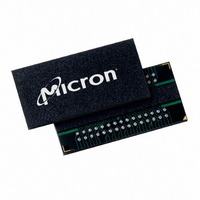
MT41J64M16LA-187E:B TR Micron Technology Inc, MT41J64M16LA-187E:B TR Datasheet - Page 156

MT41J64M16LA-187E:B TR
Manufacturer Part Number
MT41J64M16LA-187E:B TR
Description
IC DDR3 SDRAM 1GBIT 96FBGA
Manufacturer
Micron Technology Inc
Type
DDR3 SDRAMr
Specifications of MT41J64M16LA-187E:B TR
Format - Memory
RAM
Memory Type
DDR3 SDRAM
Memory Size
1G (64M x 16)
Speed
533MHz
Interface
Parallel
Voltage - Supply
1.425 V ~ 1.575 V
Operating Temperature
0°C ~ 95°C
Package / Case
96-FBGA
Organization
64Mx16
Density
1Gb
Address Bus
16b
Maximum Clock Rate
1.066GHz
Operating Supply Voltage (typ)
1.5V
Package Type
FBGA
Operating Temp Range
0C to 95C
Operating Supply Voltage (max)
1.575V
Operating Supply Voltage (min)
1.425V
Supply Current
265mA
Pin Count
96
Mounting
Surface Mount
Operating Temperature Classification
Commercial
Lead Free Status / RoHS Status
Lead free / RoHS Compliant
Other names
557-1378-2
- Current page: 156 of 208
- Download datasheet (13Mb)
Figure 71: Nonconsecutive READ Bursts
DQS, DQS#
Figure 72: READ (BL8) to WRITE (BL8)
Command 1
DQS, DQS#
Command
Address 2
Address
CK#
DQ
DQ 3
CK
CK#
CK
Bank a,
READ
Col n
T0
READ
Bank,
Col n
T0
NOP
T1
NOP
T1
READ-to-WRITE command delay = RL + t CCD + 2 t CK - WL
Notes:
Notes:
NOP
T2
NOP
T2
RL = 5
1. AL = 0, RL = 8.
2. DO n (or b) = data-out from column n (or column b).
3. Seven subsequent elements of data-out appear in the programmed order following DO n.
4. Seven subsequent elements of data-out appear in the programmed order following DO b.
1. NOP commands are shown for ease of illustration; other commands may be valid at these times.
2. The BL8 setting is activated by either MR0[1:0] = 00 or MR0[1:0] = 01 and A12 = 1 during the READ command at
3. DO n = data-out from column, DI b = data-in for column b.
4. BL8, RL = 5 (AL = 0, CL = 5), WL = 5 (AL = 0, CWL = 5).
NOP
T3
T0, and the WRITE command at T6.
NOP
T3
CL = 8
T4
NOP
NOP
T4
t RPRE
Bank a,
READ
Col b
T5
NOP
T5
DO
n
T6
NOP
n + 1
DO
WRITE
Bank,
Col b
T6
n + 2
DO
NOP
T7
n + 3
DO
NOP
T7
n + 4
DO
NOP
T8
DO
n
n + 5
DO
NOP
T8
CL = 8
n + 6
DO
NOP
T9
WL = 5
t RPST
n + 7
DO
NOP
T9
T10
NOP
NOP
T10
NOP
T11
t WPRE
NOP
T11
DI
T12
NOP
n
n + 1
DI
NOP
NOP
T12
n + 2
T13
DI
DO
b
n + 3
t BL = 4 clocks
DI
Transitioning Data
NOP
T14
NOP
T13
n + 4
DI
n + 5
DI
T15
NOP
NOP
n + 6
T14
DI
Transitioning Data
n + 7
DI
t WPST
Don’t Care
NOP
T16
NOP
T15
t WTR
t WR
NOP
Don’t Care
T17
Related parts for MT41J64M16LA-187E:B TR
Image
Part Number
Description
Manufacturer
Datasheet
Request
R

Part Number:
Description:
IC DDR3 SDRAM 1GBIT 96FBGA
Manufacturer:
Micron Technology Inc
Datasheet:

Part Number:
Description:
Manufacturer:
Micron Technology Inc
Datasheet:

Part Number:
Description:
Manufacturer:
Micron Technology Inc
Datasheet:

Part Number:
Description:
Manufacturer:
Micron Technology Inc
Datasheet:

Part Number:
Description:
IC SDRAM 64MBIT 133MHZ 54TSOP
Manufacturer:
Micron Technology Inc
Datasheet:

Part Number:
Description:
IC SDRAM 64MBIT 5.5NS 86TSOP
Manufacturer:
Micron Technology Inc
Datasheet:

Part Number:
Description:
IC SDRAM 64MBIT 200MHZ 86TSOP
Manufacturer:
Micron Technology Inc
Datasheet:

Part Number:
Description:
IC SDRAM 64MBIT 133MHZ 54TSOP
Manufacturer:
Micron Technology Inc
Datasheet:

Part Number:
Description:
IC SDRAM 128MBIT 133MHZ 54TSOP
Manufacturer:
Micron Technology Inc
Datasheet:

Part Number:
Description:
IC SDRAM 256MBIT 133MHZ 90VFBGA
Manufacturer:
Micron Technology Inc
Datasheet:

Part Number:
Description:
IC SDRAM 128MBIT 133MHZ 54TSOP
Manufacturer:
Micron Technology Inc
Datasheet:

Part Number:
Description:
IC SDRAM 256MBIT 133MHZ 54TSOP
Manufacturer:
Micron Technology Inc
Datasheet:

Part Number:
Description:
IC DDR SDRAM 512MBIT 6NS 66TSOP
Manufacturer:
Micron Technology Inc
Datasheet:

Part Number:
Description:
IC SDRAM 128MBIT 167MHZ 86TSOP
Manufacturer:
Micron Technology Inc
Datasheet:

Part Number:
Description:
IC SDRAM 128MBIT 143MHZ 86TSOP
Manufacturer:
Micron Technology Inc
Datasheet:


