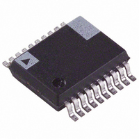
ADE7759ARSRL Analog Devices Inc, ADE7759ARSRL Datasheet - Page 12

ADE7759ARSRL
Manufacturer Part Number
ADE7759ARSRL
Description
IC ENERGY METERING 1PHASE 20SSOP
Manufacturer
Analog Devices Inc
Datasheet
1.ADE7759ARSZ.pdf
(36 pages)
Specifications of ADE7759ARSRL
Rohs Status
RoHS non-compliant
Input Impedance
390 KOhm
Measurement Error
0.1%
Voltage - I/o High
2.4V
Voltage - I/o Low
0.8V
Current - Supply
3mA
Voltage - Supply
4.75 V ~ 5.25 V
Operating Temperature
-40°C ~ 85°C
Mounting Type
Surface Mount
Package / Case
20-SSOP (0.200", 5.30mm Width)
Meter Type
Single Phase
For Use With
EVAL-ADE7759EBZ - BOARD EVALUATION FOR ADE7759
ADE7759
It is also possible to adjust offset errors on Channel 1 and
Channel 2 by writing to the offset correction registers (CH1OS
and CH2OS, respectively). These registers allow channel
offsets in the range ± 24 mV to ± 50 mV (depending on the
gain setting) to be removed. Note that it is not necessary to
perform an offset correction in an energy measurement applica-
tion if HPF1 Channel 1 is switched on. Figure 6 shows the
effect of offsets on the real power calculation; an offset on
Channel 1 and Channel 2 will contribute a dc component
after multiplication. Since this dc component is extracted by
LPF2 to generate the active (real) power information, the
offsets will have contributed an error to the active power
calculation. This problem is easily avoided by enabling HPF1
in Channel 1. By removing the offset from at least one channel,
no error component is generated at dc by the multiplication.
Error terms at cos(ω t) are removed by LPF2 and by integra-
tion of the active power signal in the active energy register
(AENERGY[39:0])—see Energy Calculation section.
The contents of the offset correction registers are 6-bit, sign and
magnitude coded. The weighting of the LSB size depends on
the gain setting, i.e., 1, 2, 4, 8, or 16. Table II shows the
correctable offset span for each of the gain settings and the LSB
weight (mV) for the offset correction registers. The maximum
value that can be written to the offset correction registers is ± 31
decimal—see Figure 7.
Gain
1
2
4
8
16
Figure 7 shows the relationship between the offset correction
register contents and the offset (mV) on the analog inputs for a
gain setting of one. To perform an offset adjustment, the analog
inputs should be first connected to AGND, and there should be
no signal on either Channel 1 or Channel 2. A read from
Channel 1 or Channel 2 using the waveform register will give an
indication of the offset in the channel. This offset can be
canceled by writing an equal but opposite offset value to the
relevant offset register. The offset correction can be confirmed
by performing another read. Note that when adjusting the offset of
Channel 1, the digital integrator and the HPF1 should be disabled.
Figure 6. Effect of Channel Offsets on the Real
Power Calculation
V
OS
V
2
I
OS
I
0
Table II. Offset Correction Range
Correctable Span
± 50 mV
± 37 mV
± 30 mV
± 26 mV
± 24 mV
DC COMPONENT (INCLUDING ERROR TERM)
IS EXTRACTED BY THE LPF FOR REAL
POWER CALCULATION
I
V
OS
OS
V
I
2
LSB Size
1.61 mV/LSB
1.19 mV/LSB
0.97 mV/LSB
0.84 mV/LSB
0.77 mV/LSB
–12–
di/dt CURRENT SENSOR AND DIGITAL INTEGRATOR
The di/dt sensor detects changes in magnetic field caused by ac
current. Figure 8 shows the principle of a di/dt current sensor.
The flux density of a magnetic field induced by a current is directly
proportional to the magnitude of the current. The changes in the
magnetic flux density passing through a conductor loop generate
an electromotive force (EMF) between the two ends of the loop.
The EMF is a voltage signal that is proportional to the di/dt of
the current. The voltage output from the di/dt current sensor
is determined by the mutual inductance between the current-
carrying conductor and the di/dt sensor. Figure 9 shows that
the mutual inductance produces a di/dt signal at the output
of the sensor.
The current signal needs to be recovered from the di/dt signal
before it can be used for active power calculation. An integrator
is therefore necessary to restore the signal to its original form.
The ADE7759 has a built-in digital integrator to recover the
current signal from the di/dt sensor. The digital integrator on
Channel 1 is switched on by default when the ADE7759 is
powered up. Setting the MSB of the CH1OS register to 0 will
turn off the integrator. Figures 10 to 13 show the magnitude
and phase response of the digital integrator.
Figure 7. Channel Offset Correction Range (Gain = 1)
Figure 9. Mutual Inductance Between the di/dt
Sensor and the Current Carrying Conductor
Figure 8. Principle of a di/dt Current Sensor
i(t)
MUTUAL INDUCTANCE M
–50mV
CH1OS[5:0]
1Fh
00h
3Fh
MAGNETIC FIELD CREATED BY CURRENT
(DIRECTLY PROPORTIONAL TO CURRENT)
0mV
01,1111b
11,1111b
+50mV
+
–
+
–
OFFSET
ADJUST
SIGN + 5 BITS
v = M
SIGN + 5 BITS
EMF (ELECTROMOTIVE FORCE)
INDUCED BY CHANGES IN
MAGNETIC FLUX DENSITY (di/dt)
di(t)
dt
REV. A


