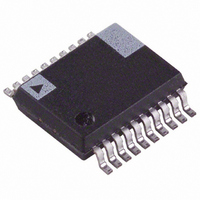
ADE7759ARSRL Analog Devices Inc, ADE7759ARSRL Datasheet - Page 19

ADE7759ARSRL
Manufacturer Part Number
ADE7759ARSRL
Description
IC ENERGY METERING 1PHASE 20SSOP
Manufacturer
Analog Devices Inc
Datasheet
1.ADE7759ARSZ.pdf
(36 pages)
Specifications of ADE7759ARSRL
Rohs Status
RoHS non-compliant
Input Impedance
390 KOhm
Measurement Error
0.1%
Voltage - I/o High
2.4V
Voltage - I/o Low
0.8V
Current - Supply
3mA
Voltage - Supply
4.75 V ~ 5.25 V
Operating Temperature
-40°C ~ 85°C
Mounting Type
Surface Mount
Package / Case
20-SSOP (0.200", 5.30mm Width)
Meter Type
Single Phase
For Use With
EVAL-ADE7759EBZ - BOARD EVALUATION FOR ADE7759
CHANNEL 2 ADC
Channel 2 Sampling
In Channel 2 waveform sampling mode (MODE[14:13] = 1, 1
and WSMP = 1), the ADC output code scaling for Channel 2 is
the same as Channel 1, i.e., the output swings between D7AE1h
(–165,151) and 2851Fh (+165,151)—see ADC Channel 1
section. However, before being passed to the waveform register,
the ADC output is passed through a single-pole, low-pass filter
with a cutoff frequency of 156 Hz. The plots in Figure 26 show
the magnitude and phase response of this filter.
The LPF1 has the effect of attenuating the signal. For example,
if the line frequency is 60 Hz, the signal at the output of LPF1
will be attenuated by 7%.
Note that LPF1 does not affect the power calculation. The
signal processing chain in Channel 2 is illustrated in Figure 27.
Unlike Channel 1, Channel 2 has only one analog input range
(0.5 V differential). However, like Channel 1, Channel 2 does
have a PGA with gain selections of 1, 2, 4, 8, and 16. For energy
measurement, the output of the ADC is passed directly to the
multiplier and is not filtered. An HPF is not required to remove
any dc offset since it is only required to remove the offset from
one channel to eliminate errors due to offsets in the power cal-
culation. When in waveform sample mode, one of four output
sample rates can be chosen by using Bits 11 and 12 of the
mode register. The available output sample rates are 27.9 kSPS,
14 kSPS, 7 kSPS, or 3.5 kSPS—see Mode Register section. The
interrupt request output IRQ signals a new sample availability
by going active low. The timing is the same as that for
Channel 1 and is shown in Figure 24.
REV. A
Figure 26. Magnitude and Phase Response of LPF1
–20
–40
–60
–80
0
10
1
H f
( )
=
60Hz, –21.04
1
+
156
FREQUENCY – Hz
60
1
Hz
Hz
10
2
2
=
0 93
60Hz, –0.6dB
.
=
– .
0 6
dB
10
3
0
–10
–20
–19–
PHASE COMPENSATION
When the HPF is disabled, the phase error between Channel 1 and
Channel 2 is zero from dc to 3.5 kHz. When HPF1 is enabled,
Channel 1 has a phase response illustrated in Figures 29 and 30.
Also shown in Figure 31 is the magnitude response of the filter.
As can be seen from the plots, the phase response is almost zero
from 45 Hz to 1 kHz. This is all that is required in typical energy
measurement applications.
However, despite being internally phase compensated, the
ADE7759 must work with transducers that may have inherent
phase errors. For example, a phase error of 0.1° to 0.3° is not
uncommon for a CT (Current Transformer). These phase
errors can vary from part to part, and they must be corrected in
order to perform accurate power calculations. The errors associ-
ated with phase mismatch are particularly noticeable at low
power factors. The ADE7759 provides a means of digitally
calibrating these small phase errors. The ADE7759 allows a
small time delay or time advance to be introduced into the signal
processing chain in order to compensate for small phase errors.
Because the compensation is in time, this technique should only be
used for small phase errors in the range of 0.1° to 0.5°. Correcting
large phase errors using a time shift technique can introduce signifi-
cant phase errors at higher harmonics.
The phase calibration register (PHCAL[7:0]) is a twos comple-
ment signed single-byte register that has values ranging from 9Eh
(–98 in decimal) to 5Ch (92 in decimal). By changing the PHCAL
register, the time delay in the Channel 2 signal path can change
from –110 µs to +103 µs (CLKIN = 3.579545 MHz). One LSB is
equivalent to 1.12 µs time delay or advance. With a line frequency
of 60 Hz, this gives a phase resolution of 0.024° at the fundamental
(i.e., 360° × 1.12 µs × 60 Hz). Figure 28 illustrates how the phase
compensation is used to remove a 0.1° phase lead in Channel 1
due to the external transducer. To cancel the lead (0.1°) in
Channel 1, a phase lead must also be introduced into Channel 2.
The resolution of the phase adjustment allows the introduction of a
phase lead in increments of 0.024°. The phase lead is achieved by
introducing a time advance into Channel 2. A time advance of
4.48 µs is made by writing –4 (FCh) to the time delay block, thus
reducing the amount of time delay by 4.48 µs, or equivalently, a
phase lead of approximately 0.1° at line frequency of 60 Hz.
0.5V, 0.25V, 0.125V,
62.5mV, 31.25mV
Figure 27. ADC and Signal Processing in Channel 2
V2
V2N
V2P
0V
V1
ANALOG
INPUT RANGE
PGA2
1,
8,
{GAIN [7:5]}
2,
16
4,
2.42V
REFERENCE
ADC 2
DA80Ah
D7AE1h
C0000h
40000h
2851Fh
257F6h
00000h
1
–63% TO +63% FS
WORD RANGE
LPF OUTPUT
LPF1
ADE7759
20
+63% FS
+59% FS
–59% FS
–63% FS
–FS
+FS
TO
MULTIPLIER
TO
WAVEFORM
REGISTER


