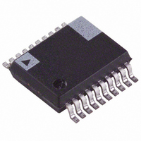
ADE7759ARSRL Analog Devices Inc, ADE7759ARSRL Datasheet - Page 29

ADE7759ARSRL
Manufacturer Part Number
ADE7759ARSRL
Description
IC ENERGY METERING 1PHASE 20SSOP
Manufacturer
Analog Devices Inc
Datasheet
1.ADE7759ARSZ.pdf
(36 pages)
Specifications of ADE7759ARSRL
Rohs Status
RoHS non-compliant
Input Impedance
390 KOhm
Measurement Error
0.1%
Voltage - I/o High
2.4V
Voltage - I/o Low
0.8V
Current - Supply
3mA
Voltage - Supply
4.75 V ~ 5.25 V
Operating Temperature
-40°C ~ 85°C
Mounting Type
Surface Mount
Package / Case
20-SSOP (0.200", 5.30mm Width)
Meter Type
Single Phase
For Use With
EVAL-ADE7759EBZ - BOARD EVALUATION FOR ADE7759
Address
0Bh
0Ch
0Dh
0Eh
0Fh
10h
11h
12h
13h
14h
15h
1Eh
1Fh
REV. A
APOS
Name
APGAIN
PHCAL
ZXTOUT
SAGCYC
IRQEN
SAGLVL
TEMP
LINECYC
LENERGY
CFNUM
CHKSUM
DIEREV
R/W No. of Bits
R/W 12
R/W 8
R/W 16
R/W 12
R/W 8
R/W 8
R/W 8
R/W 4
R
R/W 2
R
R
R
8
40
6
8
0h
0h
FFFh
FFh
40h
0h
0h
3FFFh
0h
0h
0h
01h
Default
0h
Active Power Gain Adjust. This is a 12-bit register. The active power
Zero Cross Timeout. If no zero crossings are detected on Channel 2
Sag Line Cycle Register. This 8-bit register specifies the number of
Line Cycle Energy Accumulation Mode Half-Cycle Register. This
Line Cycle Energy Accumulation Mode Active Energy Register. This
Description
calculation can be calibrated by writing to this register. The calibration
range is ±50% of the nominal full-scale active power. The resolution of the
gain adjust is 0.0244%/LSB—see Channel 1 ADC Gain Adjust section.
Phase Calibration Register. The phase relationship between Channel 1
and Channel 2 can be adjusted by writing to this 8-bit register. The
valid content of this twos complement register is between 9Eh and
5Ch, which is a phase difference of –2.365∞ to +2.221∞ at 60 Hz in
0.0241∞ steps—see Phase Compensation section.
Active Power Offset Correction. This 16-bit register allows small off-
sets in the Active Power calculation to be removed—see Active Power
Calculation section.
within a time period specified by this 12-bit register, the interrupt
request line (IRQ) will be activated. The maximum timeout period is
0.15 seconds—see Zero Crossing Detection section.
consecutive half-line cycles the signal on Channel 2 must be below
SAGLVL before the SAG output is activated—see Voltage Sag
Detection section.
Interrupt Enable Register. ADE7759 interrupts may be deactivated at
any time by setting the corresponding bit in this 8-bit enable register to
Logic 0. The status register will continue to register an interrupt event
even if disabled. However, the IRQ output will not be activated—see
Interrupts section.
Sag Voltage Level. An 8-bit write to this register determines at what
peak signal level on Channel 2 the SAG pin will become active. The
signal must remain low for the number of cycles specified in the
SAGCYC register before the SAG pin is activated—see Line Voltage
Sag Detection section.
Temperature Register. This is an 8-bit register which contains the
result of the latest temperature conversion—see Temperature
Measurement section.
14-bit register is used during line cycle energy accumulation mode to
set the number of half-line cycles active energy is accumulated—see
Line Cycle Energy Accumulation Mode section.
40-bit register accumulates active energy during line cycle energy
accumulation mode. The number of half-line cycles is set by the
LINECYC register—see Line Cycle Energy Accumulation Mode section.
CF Frequency Divider Numerator Register. The output frequency on
the CF pin is adjusted by writing to this 12-bit read/write register—see
Energy to Frequency Conversion section.
Checksum Register. This 6-bit read-only register is equal to the sum of
all the ones in the previous read—see Serial Read Operation section.
Die Revision Register. This 8-bit read-only register contains the revision
number of the silicon.
–29–
ADE7759


