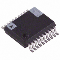
ADE7759ARSRL Analog Devices Inc, ADE7759ARSRL Datasheet - Page 28

ADE7759ARSRL
Manufacturer Part Number
ADE7759ARSRL
Description
IC ENERGY METERING 1PHASE 20SSOP
Manufacturer
Analog Devices Inc
Datasheet
1.ADE7759ARSZ.pdf
(36 pages)
Specifications of ADE7759ARSRL
Rohs Status
RoHS non-compliant
Input Impedance
390 KOhm
Measurement Error
0.1%
Voltage - I/o High
2.4V
Voltage - I/o Low
0.8V
Current - Supply
3mA
Voltage - Supply
4.75 V ~ 5.25 V
Operating Temperature
-40°C ~ 85°C
Mounting Type
Surface Mount
Package / Case
20-SSOP (0.200", 5.30mm Width)
Meter Type
Single Phase
For Use With
EVAL-ADE7759EBZ - BOARD EVALUATION FOR ADE7759
ADE7759
CHECKSUM REGISTER
The ADE7759 has a checksum register (CHKSUM[5:0]) to
ensure that the data bits received in the last serial read operation
are not corrupted. The 6-bit checksum register is reset before
the first bit (MSB of the register to be read) is put on the DOUT
pin. During a serial read operation, when each data bit becomes
available on the rising edge of SCLK, the bit will be added to
the checksum register. In the end of the serial read operation,
the content of the checksum register will be the sum of all the
ones contained in the register previously read. Using the checksum
register, the user can determine if an error has occurred during
the last read operation.
Address
01h
02h
03h
04h
05h
06h
07h
08h
09h
0Ah
Name
WAVEFORM
AENERGY
RSTENERGY R
STATUS
RSTSTATUS
MODE
CFDEN
CH1OS
CH2OS
GAIN
R/W No. of Bits Default
R
R
R
R
R/W 16
R/W 12
R/W 8
R/W 6
R/W 8
40
24/40
40
8
8
0h
0h
0h
40h
0h
000Ch
3Fh
80h
0h
0h
Table IV. Register List
Active Energy Register. Active power is accumulated (Integrated)
Same as the active energy register except that the register is reset to
Interrupt Status Register. This is an 8-bit read-only register. The
Same as the interrupt status register except that the register con-
CF Frequency Divider Denominator Register. The output fre-
Channel 1 Offset Adjust. The MSB is used to enable the digital inte-
PGA Gain Adjust. This 8-bit register is used to adjust the gain selec-
Description
The Waveform Register is a read-only register. This register con-
tains the sampled waveform data from Channel 1, Channel 2, or the
active power signal. The data source and the length of the waveform
registers are selected by data bits 14 and 13 in the mode register—
see Channel 1 and 2 Sampling section.
over time in this 40-bit, read-only register. The energy register
can hold a minimum of 11.53 seconds of active energy information
with full-scale analog inputs before it overflows—see Energy Calcu-
lation section.
0 following a read operation.
status register contains information regarding the source of
ADE7759 interrupts—see Interrupts section.
tents are reset to 0 (all flags cleared) after a read operation.
Mode Register. This is a 16-bit register through which most of
the ADE7759 functionality is accessed. Signal sample rates, filter
enabling, and calibration modes are selected by writing to this
register. The contents may be read at any time—see Mode Register
section.
quency on the CF pin is adjusted by writing to this 12-bit read/write
register—see Energy-to-Frequency Conversion section.
grator. Bit 6 is not used. Writing to Bits 0 to 5 allows offsets on
Channel 1 to be removed—see Analog Inputs section and CH1OS
Register section.
Channel 2 Offset Adjust. Writing to this 6-bit register allows any offsets
on Channel 2 to be removed—see Analog Inputs section.
tion for the PGA in Channel 1 and 2—see Analog Inputs section.
–28–
Note that a read to the CHKSUM register will also generate a
checksum of the CHKSUM register itself.
Figure 47. Checksum Register for Serial Interface Read
DOUT
+
+
CONTENT OF REGISTER (n-bytes)
CHECKSUM REGISTER ADDR: 1Eh
REV. A


