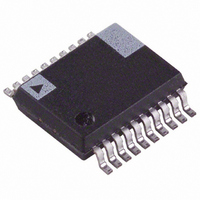
ADE7759ARSRL Analog Devices Inc, ADE7759ARSRL Datasheet - Page 27

ADE7759ARSRL
Manufacturer Part Number
ADE7759ARSRL
Description
IC ENERGY METERING 1PHASE 20SSOP
Manufacturer
Analog Devices Inc
Datasheet
1.ADE7759ARSZ.pdf
(36 pages)
Specifications of ADE7759ARSRL
Rohs Status
RoHS non-compliant
Input Impedance
390 KOhm
Measurement Error
0.1%
Voltage - I/o High
2.4V
Voltage - I/o Low
0.8V
Current - Supply
3mA
Voltage - Supply
4.75 V ~ 5.25 V
Operating Temperature
-40°C ~ 85°C
Mounting Type
Surface Mount
Package / Case
20-SSOP (0.200", 5.30mm Width)
Meter Type
Single Phase
For Use With
EVAL-ADE7759EBZ - BOARD EVALUATION FOR ADE7759
As explained earlier, the data write is initiated by a write to
the communications register followed by the data. During a
data write operation to the ADE7759, data is transferred to
all on-chip registers one byte at a time. After a byte is trans-
ferred into the serial port, there is a finite time before it is
transferred to one of the ADE7759 on-chip registers. Although
another byte transfer to the serial port can start while the
previous byte is being transferred to an on-chip register, this
second byte transfer should not finish until at least 4 µs after
the end of the previous byte transfer. This functionality is
expressed in the timing specification t
write operation is aborted during a byte transfer (CS brought
high), then that byte will not be written to the destination
register.
Destination registers may be up to 3 bytes wide—see the Regis-
ter Description section. Therefore, the first byte shifted into
the serial port at DIN is transferred to the MSB (Most Signifi-
cant Byte) of the destination register. If the addressed register
is 12 bits wide, for example, a two-byte data transfer must
take place. The data is always assumed to be right justified:
therefore, in this case, the four MSBs of the first byte would be
ignored and the four LSBs of the first byte written to the
ADE7759 would be the four MSBs of the 12-bit word. Figure 45
illustrates this example.
Serial Read Operation
During a data read operation from the ADE7759, data is shifted
out at the DOUT logic output on the rising edge of SCLK. As
REV. A
SCLK
DOUT
SCLK
DIN
DIN
CS
CS
SCLK
DIN
t
t
1
1
1
0
X
0
0
t
2
X
0
0
t
3
COMMAND BYTE
COMMAND BYTE
MOST SIGNIFICANT BYTE
A4
X
A4
6
Figure 44. Serial Interface Write Timing Diagram
Figure 46. Serial Interface Read Timing Diagram
—see Figure 44. If a
t
4
A3
A3
X
t
5
Figure 45. 12-Bit Serial Write Operation
DB11
A2
A2
A1
DB10
A1
A0
A0
DB9
t
t
7
DB8
t
11
9
–27–
was the case with the data write operation, a data read must be
preceded by a write to the communications register.
With the ADE7759 in communications mode (i.e., CS logic
low), an 8-bit write to the communications register first takes
place. The MSB of this byte transfer is a 0, indicating that the
next data transfer operation is a read. The first five LSBs of this
byte contain the address of the register that is to be read. The
ADE7759 starts shifting out of the register data on the next
rising edge of SCLK—see Figure 46. At this point, the DOUT
logic output leaves its high impedance state and starts driving
the data bus. All remaining bits of register data are shifted out
on subsequent SCLK rising edges. The serial interface also
enters communications mode again as soon as the read has been
completed. At this point, the DOUT logic output enters a high
impedance state on the falling edge of the last SCLK pulse. The
read operation may be aborted by bringing the CS logic input
high before the data transfer is complete. The DOUT output
enters a high impedance state on the rising edge of CS.
When an ADE7759 register is addressed for a read operation,
the entire contents of that register are transferred to the serial
port. This allows the ADE7759 to modify its on-chip registers
without the risk of corrupting data during a multibyte transfer.
Note that when a read operation follows a write operation, the
read command (i.e., write to communications register) should
not happen for at least 4 µs after the end of the write operation.
If the read command is sent within 4 µs of the write operation,
the last byte of the write operation may be lost. This timing
constraint is given as timing specification t
DB7
DB7
DB7
MOST SIGNIFICANT BYTE
MOST SIGNIFICANT BYTE
DB6
DB5
LEAST SIGNIFICANT BYTE
DB4
t
11
DB0
DB0
DB3
t
t
7
10
DB2
LEAST SIGNIFICANT BYTE
DB7
LEAST SIGNIFICANT BYTE
DB7
DB1
t
6
DB0
9
.
t
12
ADE7759
DB0
DB0
t
13
t
8


