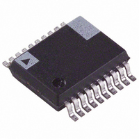
ADE7759ARSRL Analog Devices Inc, ADE7759ARSRL Datasheet - Page 8

ADE7759ARSRL
Manufacturer Part Number
ADE7759ARSRL
Description
IC ENERGY METERING 1PHASE 20SSOP
Manufacturer
Analog Devices Inc
Datasheet
1.ADE7759ARSZ.pdf
(36 pages)
Specifications of ADE7759ARSRL
Rohs Status
RoHS non-compliant
Input Impedance
390 KOhm
Measurement Error
0.1%
Voltage - I/o High
2.4V
Voltage - I/o Low
0.8V
Current - Supply
3mA
Voltage - Supply
4.75 V ~ 5.25 V
Operating Temperature
-40°C ~ 85°C
Mounting Type
Surface Mount
Package / Case
20-SSOP (0.200", 5.30mm Width)
Meter Type
Single Phase
For Use With
EVAL-ADE7759EBZ - BOARD EVALUATION FOR ADE7759
ADE7759
Pin No.
12
13
14
15
16
17
18
19
20
TERMINOLOGY
MEASUREMENT ERROR
The error associated with the energy measurement made by the
ADE7759 is defined by the following formula:
PHASE ERROR BETWEEN CHANNELS
The digital integrator and the HPF1 (High-Pass Filter) in
Channel 1 have nonideal phase response. To offset this phase
response and equalize the phase response between channels, two
phase correction networks are placed in Channel 1: one for the
digital integrator and the other for the HPF1. Each phase cor-
rection network corrects the phase response of the corresponding
component and ensures a phase match between Channel 1
(current) and Channel 2 (voltage) to within ± 0.1∞ over a range
of 45 Hz to 65 Hz and ± 0.2∞ over a range 40 Hz to 1 kHz.
POWER SUPPLY REJECTION
This quantifies the ADE7759 measurement error as a percent-
age of reading when the power supplies are varied.
For the ac PSR measurement, a reading at nominal supplies
(5 V) is taken. A second reading is obtained with the same input
signal levels when an ac (175 mV rms/120 Hz) signal is intro-
duced onto the supplies. Any error introduced by this ac signal
is expressed as a percentage of reading—see Measurement Error
definition above. For the dc PSR measurement a reading at
Percentage Error
Energy registered by the ADE
Mnemonic
ZX
SAG
IRQ
CLKIN
CLKOUT
CS
SCLK
DOUT
DIN
=
True Energy
Description
Voltage Waveform (Channel 2) Zero Crossing Output. This output toggles logic high and low at
the zero crossing of the differential signal on Channel 2—see Zero Crossing Detection section.
This open-drain logic output goes active low when either no zero crossings are detected or a low
voltage threshold (Channel 2) is crossed for a specified duration—see Line Voltage Sag Detec-
tion section.
Interrupt Request Output. This is an active low open-drain logic output. Maskable interrupts
include active energy register rollover, active energy register at half-full, zero crossing, SAG, and
arrivals of new waveform samples—see Interrupts section.
Master Clock for ADCs and Digital Signal Processing. An external clock can be provided at this
logic input. Alternatively, a parallel resonant AT crystal can be connected across CLKIN and
CLKOUT to provide a clock source for the ADE7759. The clock frequency for specified opera-
tion is 3.579545 MHz. Ceramic load capacitors of between 10 pF and 30 pF should be used with
the gate oscillator circuit. Refer to crystal manufacturer’s data sheet for load capacitance requirements.
A crystal can be connected across this pin and CLKIN as described above to provide a clock source
for the ADE7759. The CLKOUT pin can drive one CMOS load when either an external clock is
supplied at CLKIN or a crystal is being used.
Chip Select. Part of the 4-wire SPI serial interface. This active low logic input allows the ADE7759 to
share the serial bus with several other devices—see Serial Interface section.
Serial Clock Input for the Synchronous serial interface. All serial data transfers are synchronized to
this clock—see Serial Interface section. The SCLK has a Schmitt-trigger input for use with a clock
source that has a slow edge transition time, e.g., opto-isolator outputs.
Data Output for the Serial Interface. Data is shifted out at this pin on the rising edge of SCLK.
This logic output is normally in a high impedance state unless it is driving data onto the serial data
bus—see Serial Interface section.
Data Input for the Serial Interface. Data is shifted in at this pin on the falling edge of SCLK—see
Serial Interface section.
7759 –
True Energy
PIN FUNCTION DESCRIPTIONS (continued)
–8–
nominal supplies (5 V) is taken. A second reading is obtained
with the same input signal levels when the supplies are varied ± 5%.
Any error introduced is again expressed as a percentage of reading.
ADC OFFSET ERROR
This refers to the dc offset associated with the analog inputs to
the ADCs. It means that with the analog inputs connected to
AGND, the ADCs still see a dc analog input signal. The magni-
tude of the offset depends on the gain and input range selection—see
Typical Performance Characteristics. However, when HPF1 is
switched on, the offset is removed from Channel 1 (current) and
the power calculation is not affected by this offset. The offsets
may be removed by performing an offset calibration—see Analog
Inputs section.
GAIN ERROR
The gain error in the ADE7759 ADCs is defined as the difference
between the measured ADC output code (minus the offset)
and the ideal output code—see Channel 1 ADC and Channel
2 ADC. It is measured for each of the input ranges on Channel
1 (0.5 V, 0.25 V, and 0.125 V). The difference is expressed as a
percentage of the ideal code.
GAIN ERROR MATCH
The Gain Error Match is defined as the gain error (minus the
offset) obtained when switching between a gain of 1 (for each of
the input ranges) and a gain of 2, 4, 8, or 16. It is expressed as a
percentage of the output ADC code obtained under a gain of 1.
This gives the gain error observed when the gain selection is
changed from 1 to 2, 4, 8, or 16.
REV. A


