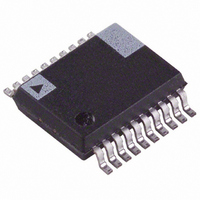
ADE7759ARSRL Analog Devices Inc, ADE7759ARSRL Datasheet - Page 5

ADE7759ARSRL
Manufacturer Part Number
ADE7759ARSRL
Description
IC ENERGY METERING 1PHASE 20SSOP
Manufacturer
Analog Devices Inc
Datasheet
1.ADE7759ARSZ.pdf
(36 pages)
Specifications of ADE7759ARSRL
Rohs Status
RoHS non-compliant
Input Impedance
390 KOhm
Measurement Error
0.1%
Voltage - I/o High
2.4V
Voltage - I/o Low
0.8V
Current - Supply
3mA
Voltage - Supply
4.75 V ~ 5.25 V
Operating Temperature
-40°C ~ 85°C
Mounting Type
Surface Mount
Package / Case
20-SSOP (0.200", 5.30mm Width)
Meter Type
Single Phase
For Use With
EVAL-ADE7759EBZ - BOARD EVALUATION FOR ADE7759
TIMING CHARACTERISTICS
Parameter
Write Timing
Read Timing
NOTES
1
2
3
4
REV. A
Sample tested during initial release and after any redesign or process change that may affect this parameter. All input signals are specified with tr = tf = 5 ns
(10% to 90%) and timed from a voltage level of 1.6 V.
See Figures 2 and 3 and Serial Interface section of this data sheet.
Measured with the load circuit in Figure 1 and defined as the time required for the output to cross 0.8 V or 2.4 V.
Derived from the measured time taken by the data outputs to change 0.5 V when loaded with the circuit in Figure 1. The measured number is then extrapolated back
to remove the effects of charging or discharging the 50 pF capacitor. This means that the time quoted in the timing characteristics is the true bus relinquish time of
the part and is independent of the bus loading.
t
t
t
t
t
t
t
t
t
t
t
t
t
1
2
3
4
5
6
7
8
9
10
11
12
13
3
4
4
SCLK
SCLK
DOUT
A, B Versions
20
150
150
10
5
6.4
4
100
4
4
30
100
10
100
10
DIN
DIN
CS
CS
t
t
1
1
1
0
t
2
0
0
Unit
ns (min)
ns (min)
ns (min)
ns (min)
ns (min)
ms (min)
ms (min)
ns (min)
ms (min)
ms (min)
ns (min)
ns (max)
ns (min)
ns (max)
ns (min)
COMMAND BYTE
COMMAND BYTE
1, 2
Figure 1. Load Circuit for Timing Specifications
0
0
t
A4
4
A4
t
3
(AV
XTAL, T
OUTPUT
A3
A3
DD
Figure 2. Serial Write Timing
Figure 3. Serial Read Timing
PIN
Test Conditions/Comments
CS Falling Edge to First SCLK Falling Edge
SCLK Logic High Pulsewidth
SCLK Logic Low Pulsewidth
Valid Data Setup Time before Falling Edge of SCLK
Data Hold Time after SCLK Falling Edge
Minimum Time between the End of Data Byte Transfers
Minimum Time between Byte Transfers during a Serial Write
CS Hold Time after SCLK Falling Edge
Minimum Time between Read Command (i.e., a Write to Communications
Register) and Data Read
Minimum Time between Data Byte Transfers during a Multibyte Read
Data Access Time after SCLK Rising Edge following a Write to the Communica-
tions Register
Bus Relinquish Time after Falling Edge of SCLK
Bus Relinquish Time after Rising Edge of CS
TO
A2
A2
= DV
t
MIN
5
A1
A1
to T
DD
50pF
= 5 V
MAX
A0
C
A0
L
= –40 C to +85 C, unless otherwise noted.)
t
t
t
11
9
7
–5–
200 A
1.6mA
5%, AGND = DGND = 0 V, On-Chip Reference, CLKIN = 3.579545 MHz
MOST SIGNIFICANT BYTE
MOST SIGNIFICANT BYTE
DB7
DB7
I
I
OL
OH
2.1V
t
11
DB0
DB0
t
t
10
7
LEAST SIGNIFICANT BYTE
LEAST SIGNIFICANT BYTE
DB7
DB7
t
6
t
12
DB0
DB0
t
13
t
8
ADE7759


