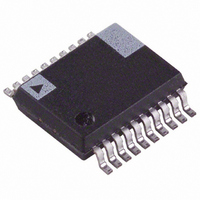
ADE7759ARSRL Analog Devices Inc, ADE7759ARSRL Datasheet - Page 26

ADE7759ARSRL
Manufacturer Part Number
ADE7759ARSRL
Description
IC ENERGY METERING 1PHASE 20SSOP
Manufacturer
Analog Devices Inc
Datasheet
1.ADE7759ARSZ.pdf
(36 pages)
Specifications of ADE7759ARSRL
Rohs Status
RoHS non-compliant
Input Impedance
390 KOhm
Measurement Error
0.1%
Voltage - I/o High
2.4V
Voltage - I/o Low
0.8V
Current - Supply
3mA
Voltage - Supply
4.75 V ~ 5.25 V
Operating Temperature
-40°C ~ 85°C
Mounting Type
Surface Mount
Package / Case
20-SSOP (0.200", 5.30mm Width)
Meter Type
Single Phase
For Use With
EVAL-ADE7759EBZ - BOARD EVALUATION FOR ADE7759
ADE7759
Table III. Frequency Dependencies of the ADE7759 Parameters
Parameter
Nyquist frequency for CH 1 and 2 ADCs CLKIN/8
PHCAL resolution (seconds per LSB)
Active Energy register update rate (Hz)
Waveform sampling rate (Number of
samples per second)
WAVSEL 1, 0 = 0 0
Maximum ZXTOUT period
SUSPENDING THE ADE7759 FUNCTIONALITY
The analog and the digital circuit can be suspended separately.
The analog portion of the ADE7759 can be suspended by set-
ting the ASUSPEND bit (Bit 4) of the mode register to logic
high—see Mode Register section. In suspend mode, all waveform
samples from the ADCs will be set to zeros. The digital circuitry
can be halted by stopping the CLKIN input and maintaining
a logic high or low on CLKIN pin. The ADE7759 can be reacti-
vated by restoring the CLKIN input and setting the ASUSPEND
bit to logic low.
APPLICATION INFORMATION
Application Note AN-564 contains detailed information on how
to design an ANSI Class 100 watt-hour meter based on the
ADE7756, a pin-to-pin compatible product with the ADE7759.
Application Note AN-578 describes an algorithm on how to
calculate the voltage and current rms values using an external
MCU. It is available from the ADE7756 product homepage
under the Application Note link on the energy metering home-
page, www.analog.com/energymeter.
SERIAL INTERFACE
All ADE7759 functionality is accessible via several on-chip regis-
ters—see Figure 41. The contents of these registers can be updated
or read using the on-chip serial interface. After power-on, or tog-
gling the RESET pin low, or a falling edge on CS, the ADE7759 is
placed in communications mode. In communications mode the
ADE7759 expects a write to its communications register. The
data written to the communications register determines whether
the next data transfer operation will be a read or a write and also
which register is accessed. Therefore, all data transfer operations
with the ADE7759, whether a read or a write, must begin with a
write to the communications register.
DOUT
Figure 41. Addressing ADE7759 Registers via the
Communications Register
DIN
0 1
1 0
1 1
REGISTER #1
REGISTER #2
REGISTER #3
REGISTER #n –1
REGISTER #n
COMMUNICATIONS
REGISTER
OUT
OUT
OUT
OUT
OUT
IN
IN
IN
IN
IN
CLKIN Dependency
4/CLKIN
CLKIN/4
CLKIN/128
CLKIN/256
CLKIN/512
CLKIN/1024
524,288/CLKIN
REGISTER
ADDRESS
DECODE
–26–
The communications register is an 8-bit wide register. The
MSB determines whether the next data transfer operation is a
read or a write. The five LSBs contain the address of the register
to be accessed. See Communications Register section for a more
detailed description. Figures 42 and 43 show the data transfer
sequences for a read and write operation, respectively.
On completion of a data transfer (read or write), the ADE7759
once again enters communications mode.
A data transfer is complete when the LSB of the ADE7759
register being addressed (for a write or a read) is transferred to
or from the ADE7759.
The serial interface of the ADE7759 is made up of four signals:
SCLK, DIN, DOUT, and CS. The serial clock for a data trans-
fer is applied at the SCLK logic input. This logic input has a
Schmitt-trigger input structure, which allows slow rising (and
falling) clock edges to be used. All data transfer operations are
synchronized to the serial clock. Data is shifted into the ADE7759
at the DIN logic input on the falling edge of SCLK. Data is
shifted out of the ADE7759 at the DOUT logic output on a
rising edge of SCLK. The CS logic input is the chip select
input. This input is used when multiple devices share the serial
bus. A falling edge on CS also resets the serial interface and
places the ADE7759 into communications mode. The CS
input should be driven low for the entire data transfer opera-
tion. Bringing CS high during a data transfer operation will
abort the transfer and place the serial bus in a high impedance
state. The CS logic input may be tied low if the ADE7759 is the
only device on the serial bus. However, with CS tied low, all
initiated data transfer operations must be fully completed, i.e.,
the LSB of each register must be transferred as there is no other
way of bringing the ADE7759 back into communications mode
without resetting the entire device, i.e., using RESET.
Serial Write Operation
The serial write sequence takes place as follows. With the
ADE7759 in communications mode (i.e., the CS input logic
low), a write to the communications register first takes place.
The MSB of this byte transfer is a 1, indicating that the data
transfer operation is a write. The first five LSBs of this byte
contain the address of the register to be written to. The ADE7759
starts shifting in the register data on the next falling edge of
SCLK. All remaining bits of register data are shifted in on the
falling edge of subsequent SCLK pulses—see Figure 44.
DOUT
SCLK
SCLK
DIN
DIN
CS
CS
Figure 43. Writing Data to the ADE7759 via the Serial
Interface
Figure 42. Reading Data from the ADE7759 via the
Serial Interface
COMMUNICATIONS REGISTER WRITE
COMMUNICATIONS REGISTER WRITE
1
0
0
0
0
0
ADDRESS
ADDRESS
MULTIBYTE READ DATA
MULTIBYTE WRITE DATA
REV. A


