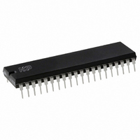
P89V51RC2FN,112 NXP Semiconductors, P89V51RC2FN,112 Datasheet - Page 17

P89V51RC2FN,112
Manufacturer Part Number
P89V51RC2FN,112
Description
IC 80C51 MCU FLASH 32K 40-DIP
Manufacturer
NXP Semiconductors
Series
89Vr
Datasheet
1.P89V51RC2FBC557.pdf
(80 pages)
Specifications of P89V51RC2FN,112
Program Memory Type
FLASH
Program Memory Size
32KB (32K x 8)
Package / Case
40-DIP (0.600", 15.24mm)
Core Processor
8051
Core Size
8-Bit
Speed
40MHz
Connectivity
SPI, UART/USART
Peripherals
Brown-out Detect/Reset, POR, PWM, WDT
Number Of I /o
32
Ram Size
1K x 8
Voltage - Supply (vcc/vdd)
4.5 V ~ 5.5 V
Oscillator Type
Internal
Operating Temperature
-40°C ~ 85°C
Processor Series
P89V5x
Core
80C51
Data Bus Width
8 bit
Data Ram Size
1 KB
Interface Type
SPI, UART
Maximum Clock Frequency
40 MHz
Number Of Programmable I/os
32
Number Of Timers
3
Operating Supply Voltage
5 V
Maximum Operating Temperature
+ 85 C
Mounting Style
SMD/SMT
3rd Party Development Tools
PK51, CA51, A51, ULINK2
Minimum Operating Temperature
- 40 C
Lead Free Status / RoHS Status
Lead free / RoHS Compliant
For Use With
622-1017 - BOARD 44-ZIF PLCC SOCKET622-1001 - USB IN-CIRCUIT PROG 80C51ISP
Eeprom Size
-
Data Converters
-
Lead Free Status / Rohs Status
Lead free / RoHS Compliant
Other names
568-2430-5
935278782112
P89V51RC2FN
935278782112
P89V51RC2FN
NXP Semiconductors
P89V51RB2_RC2_RD2_5
Product data sheet
Table 7.
Not bit addressable; Reset value 00H
Table 8.
When instructions access addresses in the upper 128 B (above 7FH), the MCU
determines whether to access the SFRs or RAM by the type of instruction given. If it is
indirect, then RAM is accessed. If it is direct, then an SFR is accessed. See the examples
below.
Indirect Access:
Register R0 points to 90H which is located in the upper address range. Data in ‘#data’ is
written to RAM location 90H rather than port 1.
Direct Access:
Data in ‘#data’ is written to port 1. Instructions that write directly to the address write to the
SFRs.
To access the expanded RAM, the EXTRAM bit must be cleared and MOVX instructions
must be used. The extra 768 B of memory is physically located on the chip and logically
occupies the first 768 B of external memory (addresses 000H to 2FFH).
When EXTRAM = 0, the expanded RAM is indirectly addressed using the MOVX
instruction in combination with any of the registers R0, R1 of the selected bank or DPTR.
Accessing the expanded RAM does not affect ports P0, P3.6 (WR), P3.7 (RD), or P2.
With EXTRAM = 0, the expanded RAM can be accessed as in the following example.
Expanded RAM Access (Indirect Addressing only):
Bit
7 to 2
1
0
Bit
Symbol
MOV@R0, #data; R0 contains 90H
MOV90H, #data; write data to P1
MOVX@DPTR, A DPTR contains 0A0H
AUXR - Auxiliary register (address 8EH) bit allocation
AUXR - Auxiliary register (address 8EH) bit description
Symbol
-
EXTRAM
AO
7
-
Rev. 05 — 12 November 2009
6
-
Description
Reserved for future use. Should be set to ‘0’ by user programs.
Internal/External RAM access using MOVX @Ri/@DPTR. When ‘0’,
core attempts to access internal XRAM with address specified in
MOVX instruction. If address supplied with this instruction exceeds
on-chip available XRAM, off-chip XRAM is going to be selected and
accessed. When ‘1’, every MOVX @Ri/@DPTR instruction targets
external data memory by default.
ALE off: disables/enables ALE. AO = 0 results in ALE emitted at a
constant rate of
active only during a MOVX or MOVC.
5
-
1
2
the oscillator frequency. In case of AO = 1, ALE is
4
P89V51RB2/RC2/RD2
-
8-bit microcontrollers with 80C51 core
3
-
2
-
EXTRAM
© NXP B.V. 2009. All rights reserved.
1
17 of 80
AO
0


