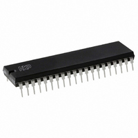
P89V51RC2FN,112 NXP Semiconductors, P89V51RC2FN,112 Datasheet - Page 60

P89V51RC2FN,112
Manufacturer Part Number
P89V51RC2FN,112
Description
IC 80C51 MCU FLASH 32K 40-DIP
Manufacturer
NXP Semiconductors
Series
89Vr
Datasheet
1.P89V51RC2FBC557.pdf
(80 pages)
Specifications of P89V51RC2FN,112
Program Memory Type
FLASH
Program Memory Size
32KB (32K x 8)
Package / Case
40-DIP (0.600", 15.24mm)
Core Processor
8051
Core Size
8-Bit
Speed
40MHz
Connectivity
SPI, UART/USART
Peripherals
Brown-out Detect/Reset, POR, PWM, WDT
Number Of I /o
32
Ram Size
1K x 8
Voltage - Supply (vcc/vdd)
4.5 V ~ 5.5 V
Oscillator Type
Internal
Operating Temperature
-40°C ~ 85°C
Processor Series
P89V5x
Core
80C51
Data Bus Width
8 bit
Data Ram Size
1 KB
Interface Type
SPI, UART
Maximum Clock Frequency
40 MHz
Number Of Programmable I/os
32
Number Of Timers
3
Operating Supply Voltage
5 V
Maximum Operating Temperature
+ 85 C
Mounting Style
SMD/SMT
3rd Party Development Tools
PK51, CA51, A51, ULINK2
Minimum Operating Temperature
- 40 C
Lead Free Status / RoHS Status
Lead free / RoHS Compliant
For Use With
622-1017 - BOARD 44-ZIF PLCC SOCKET622-1001 - USB IN-CIRCUIT PROG 80C51ISP
Eeprom Size
-
Data Converters
-
Lead Free Status / Rohs Status
Lead free / RoHS Compliant
Other names
568-2430-5
935278782112
P89V51RC2FN
935278782112
P89V51RC2FN
NXP Semiconductors
P89V51RB2_RC2_RD2_5
Product data sheet
6.13.1 Clock input options and recommended capacitor values for oscillator
6.13.2 Clock doubling option
6.13 System clock and clock options
Shown in
amplifier (XTAL1, XTAL2), which can be configured for use as an on-chip oscillator.
When driving the device from an external clock source, XTAL2 should be left disconnected
and XTAL1 should be driven.
At start-up, the external oscillator may encounter a higher capacitive load at XTAL1 due to
interaction between the amplifier and its feedback capacitance. However, the capacitance
will not exceed 15 pF once the external signal meets the V
Crystal manufacturer, supply voltage, and other factors may cause circuit performance to
differ from one application to another. C1 and C2 should be adjusted appropriately for
each design.
frequencies.
Table 57.
More specific information about on-chip oscillator design can be found in the FlashFlex51
Oscillator Circuit Design Considerations application note.
By default, the device runs at 12 clocks per machine cycle (X1 mode). The device has a
clock doubling option to speed up to 6 clocks per machine cycle (please see
Clock double mode can be enabled either by an external programmer or using IAP. When
set, the EDC bit in FST register will indicate 6-clock mode.
The clock double mode is only for doubling the internal system clock and the internal flash
memory, i.e. EA = 1. To access the external memory and the peripheral devices, careful
consideration must be taken. Also note that the crystal output (XTAL2) will not be doubled.
Crystal
Quartz
Ceramic
Fig 28. Oscillator characteristics (using the on-chip oscillator)
Figure 28
Recommended values for C1 and C2 by crystal type
Table 57
and
Rev. 05 — 12 November 2009
shows the typical values for C1 and C2 vs. crystal type for various
Figure 29
C 2
C 1
are the input and output of an internal inverting
XTAL2
XTAL1
V
SS
P89V51RB2/RC2/RD2
C1 = C2
20 pF to 30 pF
40 pF to 50 pF
8-bit microcontrollers with 80C51 core
IL
002aaa545
and V
IH
specifications.
© NXP B.V. 2009. All rights reserved.
Table
58).
60 of 80


