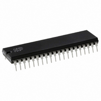
P89V51RC2FN,112 NXP Semiconductors, P89V51RC2FN,112 Datasheet - Page 62

P89V51RC2FN,112
Manufacturer Part Number
P89V51RC2FN,112
Description
IC 80C51 MCU FLASH 32K 40-DIP
Manufacturer
NXP Semiconductors
Series
89Vr
Datasheet
1.P89V51RC2FBC557.pdf
(80 pages)
Specifications of P89V51RC2FN,112
Program Memory Type
FLASH
Program Memory Size
32KB (32K x 8)
Package / Case
40-DIP (0.600", 15.24mm)
Core Processor
8051
Core Size
8-Bit
Speed
40MHz
Connectivity
SPI, UART/USART
Peripherals
Brown-out Detect/Reset, POR, PWM, WDT
Number Of I /o
32
Ram Size
1K x 8
Voltage - Supply (vcc/vdd)
4.5 V ~ 5.5 V
Oscillator Type
Internal
Operating Temperature
-40°C ~ 85°C
Processor Series
P89V5x
Core
80C51
Data Bus Width
8 bit
Data Ram Size
1 KB
Interface Type
SPI, UART
Maximum Clock Frequency
40 MHz
Number Of Programmable I/os
32
Number Of Timers
3
Operating Supply Voltage
5 V
Maximum Operating Temperature
+ 85 C
Mounting Style
SMD/SMT
3rd Party Development Tools
PK51, CA51, A51, ULINK2
Minimum Operating Temperature
- 40 C
Lead Free Status / RoHS Status
Lead free / RoHS Compliant
For Use With
622-1017 - BOARD 44-ZIF PLCC SOCKET622-1001 - USB IN-CIRCUIT PROG 80C51ISP
Eeprom Size
-
Data Converters
-
Lead Free Status / Rohs Status
Lead free / RoHS Compliant
Other names
568-2430-5
935278782112
P89V51RC2FN
935278782112
P89V51RC2FN
NXP Semiconductors
7. Limiting values
Table 61.
In accordance with the Absolute Maximum Rating System (IEC 60134).
Parameters are valid over operating temperature range unless otherwise specified. All voltages are with respect to V
otherwise noted.
8. Static characteristics
Table 62.
T
P89V51RB2_RC2_RD2_5
Product data sheet
Symbol
T
T
V
V
I
P
Symbol Parameter
n
t
I
V
V
V
V
OL(I/O)
ret(fl)
latch
a
endu(fl)
amb(bias)
stg
I
n
tot(pack)
th(HL)
th(LH)
IH
OL
= 0 C to +70 C or 40 C to +85 C; V
endurance of flash
memory
flash memory
retention time
I/O latch-up current
HIGH-LOW threshold
voltage
LOW-HIGH threshold
voltage
HIGH-level input
voltage
LOW-level output
voltage
Limiting values
Static characteristics
Parameter
bias ambient temperature
storage temperature
input voltage
voltage on any other pin
LOW-level output current per
input/output pin
total power dissipation (per package) based on package heat
Conditions
JEDEC Standard A117
JEDEC Standard A103
JEDEC Standard 78
4.5 V < V
except XTAL1, RST
4.5 V < V
V
PSEN, ALE
V
DD
DD
I
I
I
I
I
OL
OL
OL
OL
OL
= 4.5 V; ports 1, 2, 3, except
= 4.5 V; port 0, PSEN, ALE
= 100 A
= 1.6 mA
= 3.5 mA
= 200 A
= 3.2 mA
DD
DD
DD
= 4.5 V to 5.5 V; V
< 5.5 V
< 5.5 V; XTAL1, RST
Rev. 05 — 12 November 2009
Conditions
on EA pin to V
except V
V
pins P1.5, P1.6, P1.7
all other pins
transfer, not device power
consumption
DD
SS
; with respect to
SS
= 0 V
SS
[2][3][4]
P89V51RB2/RC2/RD2
[1]
[1]
[1]
8-bit microcontrollers with 80C51 core
Min
10000
100
100 + I
0.2V
0.7V
-
-
-
-
-
0.5
DD
DD
DD
+ 0.9
Min
-
-
-
55
65
0.5
0.5
Typ
-
-
-
-
-
-
-
-
-
-
-
Max
-
-
-
0.2V
V
6.0
0.3
0.45
1.0
0.3
0.45
Max
+125
+150
+14
V
20
15
1.5
DD
© NXP B.V. 2009. All rights reserved.
DD
DD
+ 0.5
+ 0.5
0.1 V
SS
Unit
cycles
years
mA
V
V
V
V
V
V
V
Unit
V
V
mA
mA
W
62 of 80
unless
C
C


