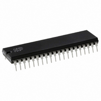
P89V51RC2FN,112 NXP Semiconductors, P89V51RC2FN,112 Datasheet - Page 63

P89V51RC2FN,112
Manufacturer Part Number
P89V51RC2FN,112
Description
IC 80C51 MCU FLASH 32K 40-DIP
Manufacturer
NXP Semiconductors
Series
89Vr
Datasheet
1.P89V51RC2FBC557.pdf
(80 pages)
Specifications of P89V51RC2FN,112
Program Memory Type
FLASH
Program Memory Size
32KB (32K x 8)
Package / Case
40-DIP (0.600", 15.24mm)
Core Processor
8051
Core Size
8-Bit
Speed
40MHz
Connectivity
SPI, UART/USART
Peripherals
Brown-out Detect/Reset, POR, PWM, WDT
Number Of I /o
32
Ram Size
1K x 8
Voltage - Supply (vcc/vdd)
4.5 V ~ 5.5 V
Oscillator Type
Internal
Operating Temperature
-40°C ~ 85°C
Processor Series
P89V5x
Core
80C51
Data Bus Width
8 bit
Data Ram Size
1 KB
Interface Type
SPI, UART
Maximum Clock Frequency
40 MHz
Number Of Programmable I/os
32
Number Of Timers
3
Operating Supply Voltage
5 V
Maximum Operating Temperature
+ 85 C
Mounting Style
SMD/SMT
3rd Party Development Tools
PK51, CA51, A51, ULINK2
Minimum Operating Temperature
- 40 C
Lead Free Status / RoHS Status
Lead free / RoHS Compliant
For Use With
622-1017 - BOARD 44-ZIF PLCC SOCKET622-1001 - USB IN-CIRCUIT PROG 80C51ISP
Eeprom Size
-
Data Converters
-
Lead Free Status / Rohs Status
Lead free / RoHS Compliant
Other names
568-2430-5
935278782112
P89V51RC2FN
935278782112
P89V51RC2FN
NXP Semiconductors
Table 62.
T
[1]
[2]
[3]
[4]
[5]
[6]
[7]
P89V51RB2_RC2_RD2_5
Product data sheet
Symbol Parameter
V
V
I
I
I
R
C
I
I
I
IL
THL
LI
DD(oper)
DD(idle)
DD(pd)
a
OH
bo
pd
iss
= 0 C to +70 C or 40 C to +85 C; V
This parameter is measured only for initial qualification and after a design or process change that could affect this parameter.
Under steady state (non-transient) conditions, I
a) Maximum I
b) Maximum I
c) If I
Capacitive loading on Ports 0 and 2 may cause spurious noise to be superimposed on the V
to external bus capacitance discharging into the Port 0 and 2 pins when the pins make 1-to-0 transitions during bus operations. In the
worst cases (capacitive loading > 100 pF), the noise pulse on the ALE pin may exceed 0.8 V. In such cases, it may be desirable to
qualify ALE with a Schmitt trigger, or use an address latch with a Schmitt trigger STROBE input.
Load capacitance for Port 0, ALE and PSEN = 100 pF, load capacitance for all other outputs = 80 pF.
Capacitive loading on Ports 0 and 2 may cause the V
the address bits are stabilizing.
Pins of Ports 1, 2 and 3 source a transition current when they are being externally driven from 1 to 0. The transition current reaches its
maximum value when V
Pin capacitance is characterized but not tested. EA = 25 pF (max).
listed test conditions.
OL
HIGH-level output
voltage
brownout trip voltage
LOW-level input
current
HIGH-LOW transition
current
input leakage current
pull-down resistance
input capacitance
operating supply
current
Idle mode supply
current
Power-down mode
supply current
Static characteristics
exceeds the test condition, V
OL
OL
per 8-bit port: 26 mA
total for all outputs: 71 mA
I
is approximately 2 V.
Conditions
V
PSEN
V
mode
V
V
0.45 V < V
on pin RST
1 MHz; T
f
f
f
f
minimum V
…continued
osc
osc
osc
osc
DD
DD
I
I
I
I
I
I
I
T
T
= 0.4 V; ports 1, 2, 3
= 2 V; ports 1, 2, 3
OH
OH
OH
OH
OH
OH
a
a
= 12 MHz
= 40 MHz
= 12 MHz
= 40 MHz
= 4.5 V; ports 1, 2, 3, ALE,
= 4.5 V; port 0 in External Bus
= 0 C to +70 C
= 40 C to +85 C
may exceed the related specification. Pins are not guaranteed to sink current greater than the
= 10 A
= 30 A
= 60 A
= 200 A
= 3.2 mA
DD
a
I
= 25 C; V
= 4.5 V to 5.5 V; V
DD
OL
< V
Rev. 05 — 12 November 2009
must be externally limited as follows:
= 2 V
DD
OH
on ALE and PSEN to momentarily fall below the V
0.3 V; port 0
I
= 0 V
SS
= 0 V
P89V51RB2/RC2/RD2
[5]
[6]
[7]
8-bit microcontrollers with 80C51 core
Min
V
V
V
V
V
3.85
-
-
-
40
-
-
-
-
-
-
-
DD
DD
DD
DD
DD
0.3
0.7
1.5
0.3
0.7
OL
of ALE and Ports 1 and 3. The noise due
Typ
-
-
-
-
-
-
-
-
-
-
-
-
-
-
-
-
-
DD
Max
-
-
-
-
-
4.15
225
15
23
50
20
42
80
90
0.7 V specification when
75
650
10
© NXP B.V. 2009. All rights reserved.
V
Unit
V
V
V
V
V
k
pF
mA
mA
mA
mA
63 of 80
A
A
A
A
A


