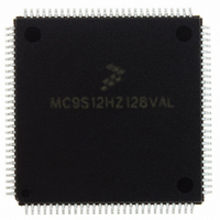
MC9S12HZ128VAL Freescale Semiconductor, MC9S12HZ128VAL Datasheet - Page 37

MC9S12HZ128VAL
Manufacturer Part Number
MC9S12HZ128VAL
Description
IC MCU 16BIT 2K FLASH 112-LQFP
Manufacturer
Freescale Semiconductor
Series
HCS12r
Datasheet
1.MC9S12HZ128CAL.pdf
(692 pages)
Specifications of MC9S12HZ128VAL
Core Processor
HCS12
Core Size
16-Bit
Speed
25MHz
Connectivity
CAN, EBI/EMI, I²C, SCI, SPI
Peripherals
LCD, Motor control PWM, POR, PWM, WDT
Number Of I /o
85
Program Memory Size
128KB (128K x 8)
Program Memory Type
FLASH
Eeprom Size
2K x 8
Ram Size
6K x 8
Voltage - Supply (vcc/vdd)
2.35 V ~ 5.5 V
Data Converters
A/D 16x10b
Oscillator Type
Internal
Operating Temperature
-40°C ~ 105°C
Package / Case
112-LQFP
Processor Series
S12H
Core
HCS12
Data Bus Width
16 bit
Data Ram Size
6 KB
Interface Type
I2C/SCI/SPI
Maximum Clock Frequency
50 MHz
Number Of Programmable I/os
85
Number Of Timers
8
Maximum Operating Temperature
+ 105 C
Mounting Style
SMD/SMT
3rd Party Development Tools
EWHCS12
Minimum Operating Temperature
- 40 C
On-chip Adc
16-ch x 10-bit
Lead Free Status / RoHS Status
Lead free / RoHS Compliant
Available stocks
Company
Part Number
Manufacturer
Quantity
Price
Company:
Part Number:
MC9S12HZ128VAL
Manufacturer:
Freescale Semiconductor
Quantity:
10 000
Part Number:
MC9S12HZ128VAL
Manufacturer:
FREESCALE
Quantity:
20 000
- Current page: 37 of 692
- Download datasheet (4Mb)
1.5
1.5.1
EXTAL and XTAL are the crystal driver and external clock pins. On reset all the device clocks are derived
from the EXTAL input frequency. XTAL is the crystal output.
1.5.2
An active low bidirectional control signal, it acts as an input to initialize the MCU to a known start-up
state, and an output when an internal MCU function causes a reset.
Freescale Semiconductor
Mnemonic
V
V
V
V
DDM1,2,3
V
V
SSM1,2,3
V
V
V
V
V
V
V
V
V
V
V
DDPLL
SSPLL
V
DDX1
DDX2
SSX1
SSX2
DDR
LCD
DD1
SSR
DDA
SSA
SS1
SS2
RH
RL
Detailed Signal Descriptions
EXTAL, XTAL — Oscillator Pins
RESET — External Reset Pin
Nominal
All V
signal transitions place high, short-duration current demands on the power
supply, use bypass capacitors with high-frequency characteristics and place
them as close to the MCU as possible. Bypass requirements depend on
MCU pin load.
Voltage
5.0 V
2.5 V
5.0 V
5.0 V
5.0 V
5.0 V
2.5 V
5.0 V
0 V
0 V
0 V
0 V
0 V
0 V
0V
SS
pins must be connected together in the application. Because fast
Voltage reference pin for the LCD driver.
Internal power and ground generated by internal regulator. These also allow an external source
to supply the core V
External power and ground, supply to pin drivers and internal voltage regulator.
External power and ground, supply to pin drivers.
Operating voltage and ground for the analog-to-digital converter and the reference for the internal
voltage regulator, allows the supply voltage to the A/D to be bypassed independently.
Reference voltage high for the ATD converter.
Reference voltage low for the ATD converter.
Provides operating voltage and ground for the phased-locked Loop. This allows the supply
voltage to the PLL to be bypassed independently. Internal power and ground generated by
internal regulator.
Provides operating voltage and ground for motor 0, 1, 2 and 3.
MC9S12HZ256 Data Sheet, Rev. 2.05
Table 1-9. Power and Ground
DD
/V
SS
voltages and bypass the internal voltage regulator.
NOTE
Description
Chapter 1 MC9S12HZ256 Device Overview
37
Related parts for MC9S12HZ128VAL
Image
Part Number
Description
Manufacturer
Datasheet
Request
R
Part Number:
Description:
Manufacturer:
Freescale Semiconductor, Inc
Datasheet:
Part Number:
Description:
Manufacturer:
Freescale Semiconductor, Inc
Datasheet:
Part Number:
Description:
Manufacturer:
Freescale Semiconductor, Inc
Datasheet:
Part Number:
Description:
Manufacturer:
Freescale Semiconductor, Inc
Datasheet:
Part Number:
Description:
Manufacturer:
Freescale Semiconductor, Inc
Datasheet:
Part Number:
Description:
Manufacturer:
Freescale Semiconductor, Inc
Datasheet:
Part Number:
Description:
Manufacturer:
Freescale Semiconductor, Inc
Datasheet:
Part Number:
Description:
Manufacturer:
Freescale Semiconductor, Inc
Datasheet:
Part Number:
Description:
Manufacturer:
Freescale Semiconductor, Inc
Datasheet:
Part Number:
Description:
Manufacturer:
Freescale Semiconductor, Inc
Datasheet:
Part Number:
Description:
Manufacturer:
Freescale Semiconductor, Inc
Datasheet:
Part Number:
Description:
Manufacturer:
Freescale Semiconductor, Inc
Datasheet:
Part Number:
Description:
Manufacturer:
Freescale Semiconductor, Inc
Datasheet:
Part Number:
Description:
Manufacturer:
Freescale Semiconductor, Inc
Datasheet:
Part Number:
Description:
Manufacturer:
Freescale Semiconductor, Inc
Datasheet:


