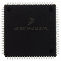
MC9S12HZ128VAL Freescale Semiconductor, MC9S12HZ128VAL Datasheet - Page 398

MC9S12HZ128VAL
Manufacturer Part Number
MC9S12HZ128VAL
Description
IC MCU 16BIT 2K FLASH 112-LQFP
Manufacturer
Freescale Semiconductor
Series
HCS12r
Datasheet
1.MC9S12HZ128CAL.pdf
(692 pages)
Specifications of MC9S12HZ128VAL
Core Processor
HCS12
Core Size
16-Bit
Speed
25MHz
Connectivity
CAN, EBI/EMI, I²C, SCI, SPI
Peripherals
LCD, Motor control PWM, POR, PWM, WDT
Number Of I /o
85
Program Memory Size
128KB (128K x 8)
Program Memory Type
FLASH
Eeprom Size
2K x 8
Ram Size
6K x 8
Voltage - Supply (vcc/vdd)
2.35 V ~ 5.5 V
Data Converters
A/D 16x10b
Oscillator Type
Internal
Operating Temperature
-40°C ~ 105°C
Package / Case
112-LQFP
Processor Series
S12H
Core
HCS12
Data Bus Width
16 bit
Data Ram Size
6 KB
Interface Type
I2C/SCI/SPI
Maximum Clock Frequency
50 MHz
Number Of Programmable I/os
85
Number Of Timers
8
Maximum Operating Temperature
+ 105 C
Mounting Style
SMD/SMT
3rd Party Development Tools
EWHCS12
Minimum Operating Temperature
- 40 C
On-chip Adc
16-ch x 10-bit
Lead Free Status / RoHS Status
Lead free / RoHS Compliant
Available stocks
Company
Part Number
Manufacturer
Quantity
Price
Company:
Part Number:
MC9S12HZ128VAL
Manufacturer:
Freescale Semiconductor
Quantity:
10 000
Part Number:
MC9S12HZ128VAL
Manufacturer:
FREESCALE
Quantity:
20 000
- Current page: 398 of 692
- Download datasheet (4Mb)
Chapter 13 Serial Communication Interface (SCIV4)
13.3.2.5
Read: anytime
Write: anytime
398
RXPOL
TXPOL
BRK13
Reset
TXDIR
Field
RAF
4
3
2
1
0
W
R
Transmit Polarity — This bit control the polarity of the transmitted data. In NRZ format, a 1 is represented by a
mark and a 0 is represented by a space for normal polarity, and the opposite for inverted polarity. In IrDA format,
a 0 is represented by short high pulse in the middle of a bit time remaining idle low for a 1 for normal polarity, and
a 0 is represented by short low pulse in the middle of a bit time remaining idle high for a 1 for inverted polarity.
0 Normal polarity
1 Inverted polarity
Receive Polarity — This bit control the polarity of the received data. In NRZ format, a 1 is represented by a mark
and a 0 is represented by a space for normal polarity, and the opposite for inverted polarity. In IrDA format, a 0
is represented by short high pulse in the middle of a bit time remaining idle low for a 1 for normal polarity, and a
0 is represented by short low pulse in the middle of a bit time remaining idle high for a 1 for inverted polarity.
0 Normal polarity
1 Inverted polarity
Break Transmit Character Length — This bit determines whether the transmit break character is 10 or 11 bit
respectively 13 or 14 bits long. The detection of a framing error is not affected by this bit.
0 Break character is 10 or 11 bit long
1 Break character is 13 or 14 bit long
Transmitter Pin Data Direction in Single-Wire Mode — This bit determines whether the TXD pin is going to
be used as an input or output, in the single-wire mode of operation. This bit is only relevant in the single-wire
mode of operation.
0 TXD pin to be used as an input in single-wire mode
1 TXD pin to be used as an output in single-wire mode
Receiver Active Flag — RAF is set when the receiver detects a logic 0 during the RT1 time period of the start
bit search. RAF is cleared when the receiver detects an idle character.
0 No reception in progress
1 Reception in progress
SCI Status Register 2 (SCISR2)
0
0
7
= Unimplemented or Reserved
0
0
6
Figure 13-8. SCI Status Register 2 (SCISR2)
Table 13-8. SCISR2 Field Descriptions
MC9S12HZ256 Data Sheet, Rev. 2.05
0
0
5
TXPOL
0
4
Description
RXPOL
0
3
BRK13
0
2
Freescale Semiconductor
TXDIR
0
1
RAF
0
0
Related parts for MC9S12HZ128VAL
Image
Part Number
Description
Manufacturer
Datasheet
Request
R
Part Number:
Description:
Manufacturer:
Freescale Semiconductor, Inc
Datasheet:
Part Number:
Description:
Manufacturer:
Freescale Semiconductor, Inc
Datasheet:
Part Number:
Description:
Manufacturer:
Freescale Semiconductor, Inc
Datasheet:
Part Number:
Description:
Manufacturer:
Freescale Semiconductor, Inc
Datasheet:
Part Number:
Description:
Manufacturer:
Freescale Semiconductor, Inc
Datasheet:
Part Number:
Description:
Manufacturer:
Freescale Semiconductor, Inc
Datasheet:
Part Number:
Description:
Manufacturer:
Freescale Semiconductor, Inc
Datasheet:
Part Number:
Description:
Manufacturer:
Freescale Semiconductor, Inc
Datasheet:
Part Number:
Description:
Manufacturer:
Freescale Semiconductor, Inc
Datasheet:
Part Number:
Description:
Manufacturer:
Freescale Semiconductor, Inc
Datasheet:
Part Number:
Description:
Manufacturer:
Freescale Semiconductor, Inc
Datasheet:
Part Number:
Description:
Manufacturer:
Freescale Semiconductor, Inc
Datasheet:
Part Number:
Description:
Manufacturer:
Freescale Semiconductor, Inc
Datasheet:
Part Number:
Description:
Manufacturer:
Freescale Semiconductor, Inc
Datasheet:
Part Number:
Description:
Manufacturer:
Freescale Semiconductor, Inc
Datasheet:


