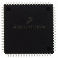
MC9S12HZ128VAL Freescale Semiconductor, MC9S12HZ128VAL Datasheet - Page 42

MC9S12HZ128VAL
Manufacturer Part Number
MC9S12HZ128VAL
Description
IC MCU 16BIT 2K FLASH 112-LQFP
Manufacturer
Freescale Semiconductor
Series
HCS12r
Datasheet
1.MC9S12HZ128CAL.pdf
(692 pages)
Specifications of MC9S12HZ128VAL
Core Processor
HCS12
Core Size
16-Bit
Speed
25MHz
Connectivity
CAN, EBI/EMI, I²C, SCI, SPI
Peripherals
LCD, Motor control PWM, POR, PWM, WDT
Number Of I /o
85
Program Memory Size
128KB (128K x 8)
Program Memory Type
FLASH
Eeprom Size
2K x 8
Ram Size
6K x 8
Voltage - Supply (vcc/vdd)
2.35 V ~ 5.5 V
Data Converters
A/D 16x10b
Oscillator Type
Internal
Operating Temperature
-40°C ~ 105°C
Package / Case
112-LQFP
Processor Series
S12H
Core
HCS12
Data Bus Width
16 bit
Data Ram Size
6 KB
Interface Type
I2C/SCI/SPI
Maximum Clock Frequency
50 MHz
Number Of Programmable I/os
85
Number Of Timers
8
Maximum Operating Temperature
+ 105 C
Mounting Style
SMD/SMT
3rd Party Development Tools
EWHCS12
Minimum Operating Temperature
- 40 C
On-chip Adc
16-ch x 10-bit
Lead Free Status / RoHS Status
Lead free / RoHS Compliant
Available stocks
Company
Part Number
Manufacturer
Quantity
Price
Company:
Part Number:
MC9S12HZ128VAL
Manufacturer:
Freescale Semiconductor
Quantity:
10 000
Part Number:
MC9S12HZ128VAL
Manufacturer:
FREESCALE
Quantity:
20 000
- Current page: 42 of 692
- Download datasheet (4Mb)
Chapter 1 MC9S12HZ256 Device Overview
1.5.6.19
PM2 is a general-purpose input or output pin. It can be configured as the receive pin RXCAN0 of the
scalable controller area network controller 0 (CAN0)
1.5.6.20
PP5 is a general-purpose input or output pin. It can be configured as pulse width modulator (PWM)
channel output PWM5 or the serial clock pin SCL of the inter-IC bus interface (IIC).
1.5.6.21
PP4 is a general-purpose input or output pin. It can be configured as pulse width modulator (PWM)
channel output PWM4 or the serial data pin SDA of the inter-IC bus interface (IIC).
1.5.6.22
PP3 is a general-purpose input or output pin. It can be configured as pulse width modulator (PWM)
channel output PWM3.
1.5.6.23
PP2 is a general-purpose input or output pin. It can be configured as pulse width modulator (PWM)
channel output PWM2 or the receive pin RXD1 of the serial communication interface 1 (SCI1).
1.5.6.24
PP1 is a general-purpose input or output pin. It can be configured as pulse width modulator (PWM)
channel output PWM1.
1.5.6.25
PP0 is a general-purpose input or output pin. It can be configured as pulse width modulator (PWM)
channel output PWM0 or the transmit pin TXD1 of the serial communication interface 1 (SCI1).
1.5.6.26
PS7 is a general-purpose input or output pin. It can be configured as slave select pin SS of the serial
peripheral interface (SPI).
1.5.6.27
PS6 is a general-purpose input or output pin. It can be configured as serial clock pin SCK of the serial
peripheral interface (SPI).
42
PM2 / RXCAN0 — Port M I/O Pin 2
PP5 / PWM5 — Port P I/O Pin 5
PP4 / PWM4 — Port P I/O Pin 4
PP3 / PWM3 — Port P I/O Pin 3
PP2 / PWM2 — Port P I/O Pin 2
PP1 / PWM1 — Port P I/O Pin 1
PP0 / PWM0 — Port P I/O Pin 0
PS7 / SS — Port S I/O Pin 7
PS6 / SCK — Port S I/O Pin 6
MC9S12HZ256 Data Sheet, Rev. 2.05
Freescale Semiconductor
Related parts for MC9S12HZ128VAL
Image
Part Number
Description
Manufacturer
Datasheet
Request
R
Part Number:
Description:
Manufacturer:
Freescale Semiconductor, Inc
Datasheet:
Part Number:
Description:
Manufacturer:
Freescale Semiconductor, Inc
Datasheet:
Part Number:
Description:
Manufacturer:
Freescale Semiconductor, Inc
Datasheet:
Part Number:
Description:
Manufacturer:
Freescale Semiconductor, Inc
Datasheet:
Part Number:
Description:
Manufacturer:
Freescale Semiconductor, Inc
Datasheet:
Part Number:
Description:
Manufacturer:
Freescale Semiconductor, Inc
Datasheet:
Part Number:
Description:
Manufacturer:
Freescale Semiconductor, Inc
Datasheet:
Part Number:
Description:
Manufacturer:
Freescale Semiconductor, Inc
Datasheet:
Part Number:
Description:
Manufacturer:
Freescale Semiconductor, Inc
Datasheet:
Part Number:
Description:
Manufacturer:
Freescale Semiconductor, Inc
Datasheet:
Part Number:
Description:
Manufacturer:
Freescale Semiconductor, Inc
Datasheet:
Part Number:
Description:
Manufacturer:
Freescale Semiconductor, Inc
Datasheet:
Part Number:
Description:
Manufacturer:
Freescale Semiconductor, Inc
Datasheet:
Part Number:
Description:
Manufacturer:
Freescale Semiconductor, Inc
Datasheet:
Part Number:
Description:
Manufacturer:
Freescale Semiconductor, Inc
Datasheet:


