MC68HC705C9ACFBE Freescale Semiconductor, MC68HC705C9ACFBE Datasheet
MC68HC705C9ACFBE
Specifications of MC68HC705C9ACFBE
Available stocks


Related parts for MC68HC705C9ACFBE


MC68HC705C9ACFBE Summary of contents
Page 1
MC68HC705C9A Advance Information Data Sheet M68HC05 Microcontrollers MC68HC705C9A Rev. 4.1 9/2005 freescale.com This document contains certain information on a new product.Specifications and information herein are subject to change without notice. ...
Page 2
Blank ...
Page 3
... September, 4.1 2005 MC68HC05C9A Advance Information Data Sheet, Rev. 4.1 Freescale Semiconductor Description Format update to current publication standards Figure 12-10. SPI Slave Timing Diagram — Corrected labels for MISO and MOSI and subtitle for part b. Figure 8-3. Timer Status Register (TSR) — Corrected address designator from $0012 to $0013 ...
Page 4
... Revision History MC68HC05C9A Advance Information Data Sheet, Rev. 4.1 4 Freescale Semiconductor ...
Page 5
... Chapter 9 Serial Communications Interface (SCI Chapter 10 Serial Peripheral Interface (SPI Chapter 11 Instruction Set . . . . . . . . . . . . . . . . . . . . . . . . . . . . . . . . . . . . . . . . . . . . . . . . . . . 79 Chapter 12 Electrical Specifications . . . . . . . . . . . . . . . . . . . . . . . . . . . . . . . . . . . . . . . . . . . 93 Chapter 13 Mechanical Specifications . . . . . . . . . . . . . . . . . . . . . . . . . . . . . . . . . . . . . . . . 107 Chapter 14 Ordering Information 111 Appendix A EPROM Programming . . . . . . . . . . . . . . . . . . . . . . . . . . . . . . . . . . . . . . . . . . . 113 Appendix B M68HC05Cx Family Feature Comparisons . . . . . . . . . . . . . . . . . . . . . . . . . . 115 MC68HC05C9A Advance Information Data Sheet, Rev. 4.1 Freescale Semiconductor 5 ...
Page 6
... List of Chapters MC68HC05C9A Advance Information Data Sheet, Rev. 4.1 6 Freescale Semiconductor ...
Page 7
... I/O Registers . . . . . . . . . . . . . . . . . . . . . . . . . . . . . . . . . . . . . . . . . . . . . . . . . . . . . . . . . . . . . . . 28 3.1 Introduction . . . . . . . . . . . . . . . . . . . . . . . . . . . . . . . . . . . . . . . . . . . . . . . . . . . . . . . . . . . . . . . . 33 3.2 CPU Registers . . . . . . . . . . . . . . . . . . . . . . . . . . . . . . . . . . . . . . . . . . . . . . . . . . . . . . . . . . . . . . 33 3.2.1 Accumulator ( 3.2.2 Index Register ( 3.2.3 Program Counter (PC 3.2.4 Stack Pointer (SP 3.2.5 Condition Code Register (CCR MC68HC05C9A Advance Information Data Sheet, Rev. 4.1 Freescale Semiconductor Chapter 1 General Description Chapter 2 Memory Chapter 3 Central Processor Unit (CPU) 7 ...
Page 8
... Port 7.3 Port 7.4 Port 7.5 Port 8.1 Introduction . . . . . . . . . . . . . . . . . . . . . . . . . . . . . . . . . . . . . . . . . . . . . . . . . . . . . . . . . . . . . . . . 51 8.2 Timer Operation . . . . . . . . . . . . . . . . . . . . . . . . . . . . . . . . . . . . . . . . . . . . . . . . . . . . . . . . . . . . . 52 8.2.1 Input Capture . . . . . . . . . . . . . . . . . . . . . . . . . . . . . . . . . . . . . . . . . . . . . . . . . . . . . . . . . . . . 52 8.2.2 Output Compare MC68HC05C9A Advance Information Data Sheet, Rev. 4.1 8 Chapter 4 Interrupts Chapter 5 Resets Chapter 6 Low-Power Modes Chapter 7 Input/Output (I/O) Ports Chapter 8 Capture/Compare Timer Freescale Semiconductor ...
Page 9
... Slave Select (SS 10.4 Functional Description . . . . . . . . . . . . . . . . . . . . . . . . . . . . . . . . . . . . . . . . . . . . . . . . . . . . . . . . 73 10.5 SPI Registers . . . . . . . . . . . . . . . . . . . . . . . . . . . . . . . . . . . . . . . . . . . . . . . . . . . . . . . . . . . . . . . 74 10.5.1 Serial Peripheral Control Register . . . . . . . . . . . . . . . . . . . . . . . . . . . . . . . . . . . . . . . . . . . . 74 10.5.2 Serial Peripheral Status Register . . . . . . . . . . . . . . . . . . . . . . . . . . . . . . . . . . . . . . . . . . . . . 76 10.5.3 Serial Peripheral Data I/O Register . . . . . . . . . . . . . . . . . . . . . . . . . . . . . . . . . . . . . . . . . . . 77 MC68HC05C9A Advance Information Data Sheet, Rev. 4.1 Freescale Semiconductor Chapter 9 Chapter 10 Serial Peripheral Interface (SPI) Table of Contents 9 ...
Page 10
... Plastic Shrink Dual In-Line (SDIP) Package (Case 858-01 108 13.4 44-Lead Plastic Leaded Chip Carrier (PLCC) (Case 777-02 109 13.5 44-Lead Quad Flat Pack (QFP) (Case 824A-01 110 MC68HC05C9A Advance Information Data Sheet, Rev. 4.1 10 Chapter 11 Instruction Set Chapter 12 Electrical Specifications Chapter 13 Mechanical Specifications Freescale Semiconductor ...
Page 11
... MC Order Numbers . . . . . . . . . . . . . . . . . . . . . . . . . . . . . . . . . . . . . . . . . . . . . . . . . . . . . . . . . 111 A.1 Introduction . . . . . . . . . . . . . . . . . . . . . . . . . . . . . . . . . . . . . . . . . . . . . . . . . . . . . . . . . . . . . . . 113 A.2 Bootloader Mode . . . . . . . . . . . . . . . . . . . . . . . . . . . . . . . . . . . . . . . . . . . . . . . . . . . . . . . . . . . 113 A.3 Bootloader Functions . . . . . . . . . . . . . . . . . . . . . . . . . . . . . . . . . . . . . . . . . . . . . . . . . . . . . . . . 113 A.4 Programming Register (PROG 114 M68HC05Cx Family Feature Comparisons MC68HC05C9A Advance Information Data Sheet, Rev. 4.1 Freescale Semiconductor Chapter 14 Ordering Information Appendix A EPROM Programming Appendix B Table of Contents 11 ...
Page 12
... Table of Contents MC68HC05C9A Advance Information Data Sheet, Rev. 4.1 12 Freescale Semiconductor ...
Page 13
... Single 3.0 volts to 5.5 volts power supply requirement • EPROM contents security 1. No security feature is absolutely secure. However, Freescale’s strategy is to make reading or copying the EPROM difficult for unauthorized users. MC68HC05C9A Advance Information Data Sheet, Rev. 4.1 Freescale Semiconductor (1) feature 13 ...
Page 14
... MISO SCI TDO RDI Figure 1-1. Block Diagram PA7 PA6 PA5 PA4 PA3 PA2 PA1 PA0 PB7 PB6 PB5 PB4 PB3 PB2 PB1 PB0 PC7 PC6 PC5 PC4 PC3 PC2 PC1 PC0 PD7 PD5/SS PD4/SCK PD3/MOSI PD2/MISO PD1/TDO PD0/RDI Freescale Semiconductor ...
Page 15
... The C9A COP reset register ($001D) and the C9A COP control register ($001E) are disabled, preventing software control over the C9A COP and clock monitor. • The C12 COP clear register ($3FF0) is enabled; this write-only register is used to clear the C12 COP. MC68HC05C9A Advance Information Data Sheet, Rev. 4.1 Freescale Semiconductor Configuration Options 15 ...
Page 16
... MC68HC05C9A Advance Information Data Sheet, Rev. 4.1 16 Figure 1-2, contains eight programmable bits which determine whether PBPU6 PBPU5 PBPU4 PBPU3 Figure 1-2. Port B Mask Option Register NOTE Figure 1-3, controls the following options: 4.3 External Interrupt (IRQ 2 1 Bit 0 PBPU2 PBPU1 PBPU0 Freescale Semiconductor ...
Page 17
... EPROM data. The EPROM data cannot be verified or modified Security enabled 0 = Security disabled During power-on reset, the device always will be configured as MC68HC05C9A regardless of the state of the C12A bit. MC68HC05C9A Advance Information Data Sheet, Rev. 4.1 Freescale Semiconductor C12COPE = Unimplemented Figure 1-3 ...
Page 18
... This bit is set by reset, but can be cleared by software. This bit can be written only once Edge and level interrupt option selected 0 = Edge-only interrupt option selected MC68HC05C9A Advance Information Data Sheet, Rev. 4.1 18 Figure 1-4, is enabled only if configured in C9A mode. This RAM1 Unimplemented Figure 1-4. C9A Option Register 2 1 Bit 0 IRQ Freescale Semiconductor ...
Page 19
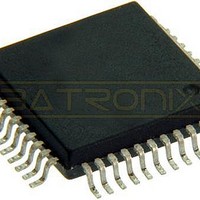
... A line over a signal name indicates an active low signal. For example, RESET is active high and RESET is active low. Figure 1-5. 40-Pin PDIP Pin Assignments MC68HC05C9A Advance Information Data Sheet, Rev. 4.1 Freescale Semiconductor Figure 1-8 show the pin assignments for the available packages. NOTE ...
Page 20
... V 3 OSC2 PP 39 PA7 4 TCAP 38 PA6 5 PD7 37 PA5 6 TCMP 36 PA4 7 PD5/SS PA3 35 8 PD4/SCK 34 PA2 9 PD3/MOSI 33 PA1 10 PD2/MISO 32 PA0 11 PD1/TDO 31 PB0 12 PD0/RDI 30 PB1 13 PC0 29 PB2 14 PC1 28 PB3 15 PC2 27 N/C 16 N/C 26 PB4 17 PC3 25 PB5 18 PC4 24 PB6 19 PC5 23 PB7 20 PC6 PC7 SS Freescale Semiconductor ...
Page 21
... MC68HC05C9A. To allow compatibility with the 44-pin PLCC MC68HC05C12A, pin17 and pin18 must be tied together and pin 39 and pin 40 also must be tied together. To allow compatibility with MC68HC705C8A, pin 3 and pin 4 also should be tied together. MC68HC05C9A Advance Information Data Sheet, Rev. 4.1 Freescale Semiconductor Functional Pin Descriptions 1 N/C 39 TCMP ...
Page 22
... These pins provide control input for an on-chip clock oscillator circuit. A crystal connected to these pins provides a system clock. The internal frequency is one-half the crystal frequency. MC68HC05C9A Advance Information Data Sheet, Rev. 4.1 22 TCMP 33 PD5/SS 32 PD4/SCK 31 PD3/MOSI 30 PD2/MISO 29 PD1/TDO 28 PD0/RDI 27 PC0 26 PC1 25 PC2 24 PC3 23 is the positive supply and V DD Freescale Semiconductor is ground. SS should be tied PP ...
Page 23
... D pins are configured as inputs during reset. When configured as a C12A, the port D pins are input only. Refer to MC68HC05C9A Advance Information Data Sheet, Rev. 4.1 Freescale Semiconductor for more detail. Chapter 7 Input/Output (I/O) Ports Chapter 7 Input/Output (I/O) Ports for more detail ...
Page 24
... General Description MC68HC05C9A Advance Information Data Sheet, Rev. 4.1 24 Freescale Semiconductor ...
Page 25
... When configured as a C9A, an additional 3,840 bytes of user EPROM from $0100 to $0FFF are enabled. Locations $3FF0 and $3FF1 are the mask option registers (MOR) (see For detailed information on programming the EPROM see MC68HC05C9A Advance Information Data Sheet, Rev. 4.1 Freescale Semiconductor NOTE Figure 2-1 and Figure 2-2 ...
Page 26
... UNUSED $001D $001E $001F UNUSED $3FF0 $3FF1 $3FF2 $3FF3 $3FF4 $3FF5 $3FF6 $3FF7 $3FF8 $3FF9 $3FFA $3FFB $3FFC $3FFD $3FFE $3FFF Freescale Semiconductor ...
Page 27
... MASK OPTION REGISTERS $3FF1 $3FF2 USER EPROM VECTORS 14 BYTES $3FFF MC68HC05C9A Advance Information Data Sheet, Rev. 4.1 Freescale Semiconductor PORT A DATA REGISTER PORT B DATA REGISTER PORT C DATA REGISTER PORT D DATA REGISTER PORT A DATA DIRECTION REGISTER PORT B DATA DIRECTION REGISTER PORT C DATA DIRECTION REGISTER ...
Page 28
... A summary of these registers is shown in given Figure 2-4. MC68HC05C9A Advance Information Data Sheet, Rev. 4.1 28 NOTE Appendix A EPROM Figure 2-3. More detail about the contents of these registers is Programming. Freescale Semiconductor ...
Page 29
... MC68HC05C9A Advance Information Data Sheet, Rev. 4.1 Freescale Semiconductor Register Name Port A Data Register Port B Data Register Port C Data Register Port D Data Register Port A Data Direction Register Port B Data Direction Register Port C Data Direction Register ...
Page 30
... DDRA2 DDRA1 DDRB4 DDRB3 DDRB2 DDRB1 DDRC4 DDRC3 DDRC2 DDRC1 DDRC4 DDRC3 DDRC2 DDRC1 MSTR CPOL CPHA SPR1 MODF SPD4 SPD3 SPD2 SPD1 Unaffected by reset R = Reserved U = Unaffected Freescale Semiconductor Bit 0 PA0 PB0 PC0 PD0 DDRA0 0 DDRB0 0 DDRC0 0 DDRC0 0 SPR0 U 0 SPD0 ...
Page 31
... High (OCRH) See page 56. Output Compare Register $0017 Low (OCRL) See page 56. Timer Register High $0018 (TRH) See page 55. Figure 2-4. Input/Output Registers (Sheet MC68HC05C9A Advance Information Data Sheet, Rev. 4.1 Freescale Semiconductor Bit Read: SCP1 Write: Reset: — — 0 Read: ...
Page 32
... Read Write: Reset Unimplemented Bit 4 Bit 3 Bit 2 Bit Bit 12 Bit 11 Bit 10 Bit Bit 4 Bit 3 Bit 2 Bit LATCH Bit 4 Bit 3 Bit 2 Bit COPF CME COPE CM1 Reserved U = Unaffected Freescale Semiconductor Bit 0 Bit 0 0 Bit 8 1 Bit 0 0 EPGM 0 Bit 0 0 CM0 0 R ...
Page 33
... This section contains the basic programmers model and the registers contained in the CPU. 3.2 CPU Registers The MCU contains five registers as shown in the programming model of order is shown in Figure 3- INCREASING MEMORY ADDRESSES UNSTACK MC68HC05C9A Advance Information Data Sheet, Rev. 4.1 Freescale Semiconductor CCR Figure 3-1 ...
Page 34
... When set, this bit indicates that a carry or borrow out of the arithmetic logical unit (ALU) occurred during the last arithmetic operation. This bit is also affected during bit test and branch instructions and during shifts and rotates. MC68HC05C9A Advance Information Data Sheet, Rev. 4.1 34 Freescale Semiconductor ...
Page 35
... SWI was fetched, but before interrupts generated after the SWI was fetched. The interrupt service routine address is specified by the contents of memory locations $3FFC and $3FFD. MC68HC05C9A Advance Information Data Sheet, Rev. 4.1 Freescale Semiconductor NOTE Figure 4-1 shows the interrupt ...
Page 36
... None I bit ICIE bit OCIE bit I bit TOIE bit TCIE bit I bit RIE bit ILIE bit SPIE I bit NOTE Vector Address 1 $3FFE–$3FFF $3FFC–$3FFD 2 $3FFA–$3FFB 3 $3FF8–$3FF9 4 $3FF6–$3FF7 5 $3FF4–$3FF5 Freescale Semiconductor ...
Page 37
... Y Y RESTORE REGISTERS FROM STACK: CCR,A,X,PC MC68HC05C9A Advance Information Data Sheet, Rev. 4.1 Freescale Semiconductor FROM RESET I BIT IN CCR SET? N CLEAR IRQ IRQ OR PORT B Y REQUEST EXTERNAL LATCH INTERRUPT N INTERNAL Y TIMER INTERRUPT N INTERNAL Y SCI INTERRUPT N INTERNAL Y SPI INTERRUPT N FETCH NEXT INSTRUCTION ...
Page 38
... SPI status register (SPSR), and the enable bits are in the SPI control register (SPCR). Either of these interrupts will vector to the same interrupt service routine, located at the address specified by the contents of memory locations $3FF4 and $3FF5. MC68HC05C9A Advance Information Data Sheet, Rev. 4.1 38 Freescale Semiconductor ...
Page 39
... MC68HC05C9A configuration the pin is bidirectional. In both cases the MCU is reset when a logic 0 is applied to the RESET pin for a period of one and one-half machine cycles (t configuration, the RESET pin will be driven low by a COP, clock monitor, or power-on reset. MC68HC05C9A Advance Information Data Sheet, Rev. 4.1 Freescale Semiconductor CLOCK MONITOR COP WATCHDOG POWER-ON RESET ...
Page 40
... C12COPE bit in the C12A mask option register (C12MOR). The function and control of both COPs is detailed below. MC68HC05C9A Advance Information Data Sheet, Rev. 4.1 40 NEW NEW 3FFE 3FFE DUMMY CODE Figure 5-2. Power-On Reset and RESET NEW NEW 3FFE 3FFE 3FFF DUMMY PCH PCL CODe Freescale Semiconductor ...
Page 41
... Selects timeout duration of COP timer and flags the following conditions: • A COP timeout • Clock monitor reset MC68HC05C9A Advance Information Data Sheet, Rev. 4.1 Freescale Semiconductor Figure 5-3 shows a block diagram of the MC68HC05C9A COP. ÷2 ÷2 ÷2 ÷2 ÷2 ÷2 ÷2 ÷ ÷4 ÷ ...
Page 42
... MC68HC05C9A Advance Information Data Sheet, Rev. 4 COPF CME Undetermined Table 5-1. COP Timeout Period Timeout Period Divide 2.0 MHz) osc 1 32. 131. 524. 2.097 sec 2 1 Bit 0 COPE CM1 CM0 Timeout Period (f = 4.0 MHz) osc 16.38 ms 65.54 ms 262.14 ms 1.048 sec Freescale Semiconductor ...
Page 43
... RESET pin for four bus cycles if the clock is slow or until the clocks recover in the case where the clocks are absent. MC68HC05C9A Advance Information Data Sheet, Rev. 4.1 Freescale Semiconductor MC68HC05C12A Compatible COP Clear Register Figure 5-6, resets the C12A COP counter. ...
Page 44
... C12MOR. Stop mode will not actually be disabled as on the MC68HC05C12A, but the clock monitor circuit will be activated. If the CPU executes a STOP instruction, the clock monitor will provide a system reset. This feature cannot be used with operating frequencies of 200 kHz or less. MC68HC05C9A Advance Information Data Sheet, Rev. 4.1 44 NOTE Freescale Semiconductor ...
Page 45
... Notes: 1. Represents the internal gating of the OSC1 pin 2. IRQ pin edge-sensitive mask option 3. IRQ pin level and edge-sensitive mask option Figure 6-1. Stop Recovery Timing Diagram MC68HC05C9A Advance Information Data Sheet, Rev. 4.1 Freescale Semiconductor LIH t ILCH 4064 t cyc 3FFE 3FFE ...
Page 46
... During wait mode, the I bit in the CCR is cleared to enable interrupts. All other registers, memory, and input/output lines remain in their previous state. The timer, SCI, and SPI may be enabled to allow a periodic exit from the wait mode. MC68HC05C9A Advance Information Data Sheet, Rev. 4.1 46 Freescale Semiconductor ...
Page 47
... Writing DDR bit sets the corresponding port bit to output mode. A block diagram of the port logic is shown in Figure 7-1. INTERNAL HC05 CONNECTIONS MC68HC05C9A Advance Information Data Sheet, Rev. 4.1 Freescale Semiconductor NOTE DATA DIRECTION REGISTER BIT LATCHED OUTPUT DATA BIT INPUT REG ...
Page 48
... SCI and SPI subsystems are disabled, thereby returning the ports to inputs. Writing DDR bit sets the corresponding port bit to output mode only when configured as a C9A. MC68HC05C9A Advance Information Data Sheet, Rev. 4.1 48 Figure 7-1 is also applicable to port C. Freescale Semiconductor ...
Page 49
... WRITE $0001 READ $0001 SOFTWARE OR MASK OPTION REGISTER CONTROLLED DEPENDENT ON CONFIGURATION FROM OTHER PORT B PINS IRQ RESET EXTERNAL INTERRUPT VECTOR FETCH MC68HC05C9A Advance Information Data Sheet, Rev. 4.1 Freescale Semiconductor V DD DISABLED ENABLED DATA DIRECTION REGISTER B BIT DDRB7 PORT B DATA REGISTER ...
Page 50
... Input/Output (I/O) Ports MC68HC05C9A Advance Information Data Sheet, Rev. 4.1 50 Freescale Semiconductor ...
Page 51
... REGISTER OUTPUT COMPARE CIRCUIT TIMER STATUS ICF OCF TOF $13 REG. INTERRUPT CIRCUIT Figure 8-1. Capture/Compare Timer Block Diagram MC68HC05C9A Advance Information Data Sheet, Rev. 4.1 Freescale Semiconductor INTERNAL BUS INTERNAL PROCESSOR 8-BIT CLOCK BUFFER ³³³ ÷4 HIGH LOW BYTE ...
Page 52
... Timer status register (TSR) • Timer registers (TRH and TRL) • Alternate timer registers (ATRH and ATRL) • Input capture registers (ICRH and ICRL) • Output compare registers (OCRH and OCRL) MC68HC05C9A Advance Information Data Sheet, Rev. 4.1 52 Freescale Semiconductor ...
Page 53
... The state of this read/write bit determines whether a logic 1 or logic 0 appears on the TCMP pin when a successful output compare occurs. Resets clear the OLVL bit TCMP goes high on output compare 0 = TCMP goes low on output compare MC68HC05C9A Advance Information Data Sheet, Rev. 4.1 Freescale Semiconductor Figure 8-2, performs these functions ...
Page 54
... TOF bit by reading the timer status register with TOF set, and then reading the low byte ($0019) of the timer registers. Resets have no effect on TOF. MC68HC05C9A Advance Information Data Sheet, Rev. 4.1 54 Figure 8-3, contains flags to signal the following conditions OCF TOF Unimplemented U = Undetermined Figure 8-3. Timer Status Register (TSR Bit Freescale Semiconductor ...
Page 55
... To prevent interrupts from occurring between readings of ATRH and ATRL, set the interrupt flag in the condition code register before reading ATRH, and clear the flag after reading ATRL. MC68HC05C9A Advance Information Data Sheet, Rev. 4.1 Freescale Semiconductor Figure 8-4, contains the current high and low bytes of the 6 ...
Page 56
... Unaffected by reset Bit 6 Bit 5 Bit 4 Bit 3 Unaffected by reset = Unimplemented NOTE Bit 14 Bit 13 Bit 12 Bit 11 Unaffected by reset Bit 6 Bit 5 Bit 4 Bit 3 Unaffected by reset 2 1 Bit 0 Bit 10 Bit 9 Bit Bit 0 Bit 2 Bit 1 Bit Bit 0 Bit 10 Bit 9 Bit Bit 0 Bit 2 Bit 1 Bit 0 Freescale Semiconductor ...
Page 57
... If reset is used to exit stop mode, then no input capture flag or data remains, even if a valid input capture edge occurred. MC68HC05C9A Advance Information Data Sheet, Rev. 4.1 Freescale Semiconductor Timer During Wait Mode 57 ...
Page 58
... Capture/Compare Timer MC68HC05C9A Advance Information Data Sheet, Rev. 4.1 58 Freescale Semiconductor ...
Page 59
... Features of the SCI receiver include: • Receiver wakeup function (idle line or address bit) • Idle line detection • Framing error detection • Noise detection • Overrun detection • Receiver data register full flag MC68HC05C9A Advance Information Data Sheet, Rev. 4.1 Freescale Semiconductor 59 ...
Page 60
... SCSR $0010 RDRF IDLE SBK FLAG RECEIVER CONTROL CONTROL WAKE NOTE RECEIVE $0011 DATA REGISTER $000F SCCR2 TIE 7 RECEIVE TCIE 6 DATA SHIFT RIE 5 REGISTER ILIE SBK 1 RWU 0 1 WAKEUP UNIT RECEIVER CLOCK 1 0 SCCR1 $000E Freescale Semiconductor RDI PIN ...
Page 61
... OSC FREQ ³÷ OSC MC68HC05C9A Advance Information Data Sheet, Rev. 4.1 Freescale Semiconductor Figure 9-1. Option bits in serial control register1 (SCCR1) select Figure 9-2). All data is transmitted least significant bit SCP0–SCP1 SCR0–SCR2 SCI PRESCALER ...
Page 62
... MC68HC05C9A Advance Information Data Sheet, Rev. 4 used and must meet the following criteria: CONTROL BIT M SELECTS 8- OR 9-BIT DATA START Figure 9-3. Data Format NOTE 0 STOP START Freescale Semiconductor ...
Page 63
... IDLE RDI RDI NOISE RDI Figure 9-4. SCI Examples of Start Bit Sampling Techniques PREVIOUS BIT RDI 16RT 1RT Figure 9-5. SCI Sampling Technique Used on All Bits MC68HC05C9A Advance Information Data Sheet, Rev. 4.1 Freescale Semiconductor Figure 9-6. 1RT START START START 0 ...
Page 64
... Case 1: Receive line low during artificial edge EXPECTED STOP START EDGE DATA SAMPLES START QUALIFIERS DATA SAMPLES Figure 9-6); therefore, the start bit will DATA START BIT DATA START BIT DETECTED AS VALID START EDGE START BIT START EDGE VERIFICATION SAMPLES Freescale Semiconductor ...
Page 65
... When the SCI is receiving 9-bit characters the ninth bit of the received character. R8 receives the ninth bit at the same time that the SCDR receives the other eight bits. Resets have no effect on the R8 bit. MC68HC05C9A Advance Information Data Sheet, Rev. 4.1 Freescale Semiconductor 9.6 Data Format and shown in Figure ...
Page 66
... This read/write bit enables SCI interrupt requests when the TC flag becomes set. Resets clear the TCIE bit interrupt requests enabled interrupt requests disabled MC68HC05C9A Advance Information Data Sheet, Rev. 4.1 66 Figure 9-10, has these functions TCIE RIE ILIE Bit 0 RE RWU SBK Freescale Semiconductor ...
Page 67
... Transmission complete • Transfer of receive shift register data SCDR complete • Receiver input idle • Noisy data • Framing error MC68HC05C9A Advance Information Data Sheet, Rev. 4.1 Freescale Semiconductor Figure 9-11, contains flags to signal the following conditions: SCI I/O Registers 67 ...
Page 68
... This clearable, read-only flag is set when noise is detected in data received in the SCI data register. Clear the NF bit by reading the SCSR and then reading the SCDR Noise detected in SCDR noise detected in SCDR MC68HC05C9A Advance Information Data Sheet, Rev. 4 RDRF IDLE Figure 9-11. SCI Status Register (SCSR Bit — Freescale Semiconductor ...
Page 69
... These read/write bits select the SCI baud rate, as shown in SCR2–SCR0 bits. SCR[2:0] 000 001 010 011 100 101 110 111 MC68HC05C9A Advance Information Data Sheet, Rev. 4.1 Freescale Semiconductor Figure 9-12, selects the baud rate for both the receiver and the SCP1 SCP0 — — ...
Page 70
... Serial Communications Interface (SCI) MC68HC05C9A Advance Information Data Sheet, Rev. 4.1 70 Freescale Semiconductor ...
Page 71
... If this bit is clear, the line is disconnected from the SPI logic and becomes a general-purpose input line. When the SPI is enabled, any SPI input line is forced to act as an input regardless of what is in the corresponding data direction register bit. MC68HC05C9A Advance Information Data Sheet, Rev. 4.1 Freescale Semiconductor NOTE 71 ...
Page 72
... SS pin is pulled low during a transmission, a mode fault error flag (MODF) is set in MC68HC05C9A Advance Information Data Sheet, Rev. 4 INTERNAL STROBE FOR DATA CAPTURE (ALL MODES) Figure 10-1. Data Clock Timing Diagram CPOL = 0 CPHA = 0 CPOL = 0 CPHA = 1 CPOL = 1 CPHA = 0 CPOL = 1 CPHA = Freescale Semiconductor ...
Page 73
... SELECT SPR1 SPR0 SPI CONTROL REGISTER (SPCR) SPI STATUS REGISTER (SPSR) SPI DATA REGISTER (SPDR) Figure 10-2. Serial Peripheral Interface Block Diagram MC68HC05C9A Advance Information Data Sheet, Rev. 4.1 Freescale Semiconductor SPI SHIFT REGISTER SPDR ($000C) SPIE SPIF SPE WCOL MSTR ...
Page 74
... Controls the clock/data relationship between master and slave • Determines the idle level of the clock pin MC68HC05C9A Advance Information Data Sheet, Rev. 4.1 74 PD3/MOSI SPI SHIFT REGISTER PD2/MISO PD5/SS I/O PORT SPDR ($000C) PD4/SCK SLAVE MCU Figure 10-4, controls these functions: Freescale Semiconductor ...
Page 75
... SCK invokes the first data sample. When CPHA=1, the SS pin may be thought simple output enable control. See SPR1 and SPR0 — SPI Clock Rate Selects These read/write bits select one of four master mode serial clock rates, as shown in have no effect in the slave mode. MC68HC05C9A Advance Information Data Sheet, Rev. 4.1 Freescale Semiconductor DWOM ...
Page 76
... Table 10-1. SPI Clock Rate Selection SPI Clock Rate Internal Clock ÷ Internal Clock ÷ Internal Clock ÷ Internal Clock ÷ Figure 10-5, contains flags to signal the following conditions WCOL MODF Unimplemented Figure 10-5. SPI Status Register 2 1 Bit Freescale Semiconductor ...
Page 77
... A write to the serial peripheral data I/O register is not buffered and places data directly into the shift register for transmission. $000C Bit 7 Read: SPD7 Write: Reset: MC68HC05C9A Advance Information Data Sheet, Rev. 4.1 Freescale Semiconductor Figure 10-6, is used to transmit and receive data SPD6 SPD5 ...
Page 78
... Serial Peripheral Interface (SPI) MC68HC05C9A Advance Information Data Sheet, Rev. 4.1 78 Freescale Semiconductor ...
Page 79
... Direct instructions can access any of the first 256 memory locations with two bytes. The first byte is the opcode, and the second is the low byte of the operand address. In direct addressing, the CPU automatically uses $00 as the high byte of the operand address. MC68HC05C9A Advance Information Data Sheet, Rev. 4.1 Freescale Semiconductor 79 ...
Page 80
... When using the Freescale assembler, the programmer does not need to calculate the offset, because the assembler determines the proper offset and verifies that it is within the span of the branch. MC68HC05C9A Advance Information Data Sheet, Rev. 4.1 80 Freescale Semiconductor ...
Page 81
... Multiply OR Accumulator with Memory Byte Subtract Memory Byte and Carry Bit from Accumulator Store Accumulator in Memory Store Index Register in Memory Subtract Memory Byte from Accumulator MC68HC05C9A Advance Information Data Sheet, Rev. 4.1 Freescale Semiconductor Instruction Instruction Types Mnemonic ADC ADD AND ...
Page 82
... BSET use only direct addressing. 2. TST is an exception to the read-modify-write sequence because it does not write a replacement value. MC68HC05C9A Advance Information Data Sheet, Rev. 4.1 82 NOTE Instruction Mnemonic ASL ASR BCLR BSET CLR COM DEC INC LSL LSR NEG ROL ROR TST (1) (1) (2) Freescale Semiconductor ...
Page 83
... Branch if Interrupt Mask Set Branch if Not Equal Branch if Plus Branch Always Branch if Bit Clear Branch Never Branch if Bit Set Branch to Subroutine Unconditional Jump Jump to Subroutine MC68HC05C9A Advance Information Data Sheet, Rev. 4.1 Freescale Semiconductor Instruction Mnemonic BCC BCS BEQ BHCC BHCS BHI BHS BIH ...
Page 84
... Transfer Index Register to Accumulator Stop CPU Clock and Enable Interrupts MC68HC05C9A Advance Information Data Sheet, Rev. 4.1 84 Instruction Table 11-5. Control Instructions Instruction Mnemonic BCLR BRCLR BRSET BSET Mnemonic CLC CLI NOP RSP RTI RTS SEC SEI STOP SWI TAX TXA WAIT Freescale Semiconductor ...
Page 85
... BHI rel Branch if Higher BHS rel Branch if Higher or Same BIH rel Branch if IRQ Pin High BIL rel Branch if IRQ Pin Low MC68HC05C9A Advance Information Data Sheet, Rev. 4.1 Freescale Semiconductor Effect on CCR Description ← (A) + (M) + (C) — A ← (A) + (M) — A ← (A) ∧ (M) — ...
Page 86
... F5 3 REL REL REL REL REL REL REL REL DIR (b0 DIR (b1 DIR (b2 DIR (b3 DIR (b4 DIR (b5 DIR (b6 DIR (b7 REL DIR (b0 DIR (b1 DIR (b2 DIR (b3 DIR (b4 DIR (b5 DIR (b6 DIR (b7 DIR (b0 DIR (b1 DIR (b2 DIR (b3 DIR (b4 DIR (b5 DIR (b6 DIR (b7 REL INH 98 2 INH 9A 2 Freescale Semiconductor ...
Page 87
... JMP opr,X Unconditional Jump JMP opr,X JMP ,X JSR opr JSR opr JSR opr,X Jump to Subroutine JSR opr,X JSR ,X MC68HC05C9A Advance Information Data Sheet, Rev. 4.1 Freescale Semiconductor Effect on CCR Description ← $00 A ← $00 X ← $00 — — — M ← $00 M ← $00 (A) – ...
Page 88
... DIR 34 5 INH 44 3 INH 54 3 IX1 INH DIR 30 5 INH 40 3 INH 50 3 IX1 INH IMM DIR EXT CA 4 — IX2 IX1 DIR 39 5 INH 49 3 INH 59 3 IX1 DIR 36 5 INH 46 3 INH 56 3 IX1 INH 9C 2 Freescale Semiconductor ...
Page 89
... Transfer Accumulator to Index Register TST opr TSTA TSTX Test Memory Byte for Negative or Zero TST opr,X TST ,X MC68HC05C9A Advance Information Data Sheet, Rev. 4.1 Freescale Semiconductor Effect on CCR Description ← (SP Pull (CCR) SP ← (SP Pull (A) SP ← (SP Pull (X) SP ← (SP Pull (PCH) SP ← ...
Page 90
... Relative program counter offset byte SP Stack pointer X Index register Z Zero flag # Immediate value ∧ Logical AND ∨ Logical OR ⊕ Logical EXCLUSIVE Contents of –( ) Negation (two’s complement) ← Loaded with ? If : Concatenated with Set or cleared — Not affected Freescale Semiconductor INH 9F 2 INH 8F 2 ...
Page 91
Bit Manipulation Branch Read-Modify-Write DIR DIR REL DIR INH MSB LSB BRSET0 BSET0 BRA NEG NEGA 3 DIR 2 DIR 2 REL 2 DIR BRCLR0 ...
Page 92
... Instruction Set MC68HC05C9A Advance Information Data Sheet, Rev. 4.1 92 Freescale Semiconductor ...
Page 93
... Thermal Characteristics Characteristic Thermal resistance plastic dual in-line (PDIP) Thermal resistance plastic leaded chip carrier (PLCC) Thermal resistance quad flat pack (QFP) Thermal resistance plastic shrink DIP (SDIP) MC68HC05C9A Advance Information Data Sheet, Rev. 4.1 Freescale Semiconductor Symbol and NOTE Symbol ...
Page 94
... Using this value of K, the values SEE TABLE TEST POINT C R1 (SEE TABLE) (SEE TABLE PA7–PA0 PB7–PB0 2.38 Ω PC7–PC0 PD5–PD0, PD7 Figure 12-1. Test Load (neglecting and T can 3.0 V Pins R1 R2 10.91 Ω 6.32 Ω Freescale Semiconductor (1) (2) ( ...
Page 95
... I/O pins configured as inputs, port 0 –0 loads; less than all outputs the OSC2 capacitance. 5. Stop I measured with OSC1 = 0.2 V; all I/O pins configured as inputs, port –0 Input pullup current measured with V MC68HC05C9A Advance Information Data Sheet, Rev. 4.1 Freescale Semiconductor (1) Symbol ...
Page 96
... OSC2 L , all other inputs OSC2. Wait I is affected linearly all other inputs Freescale Semiconductor Unit µA µA µA µA µA µ all DD ...
Page 97
... Figure 12-2. Maximum Supply Current vs Internal Clock Frequency, V Figure 12-3. Maximum Supply Current vs Internal Clock Frequency, V MC68HC05C9A Advance Information Data Sheet, Rev. 4.1 Freescale Semiconductor 50 µA 0.5 MHz 1.0 MHz 1.5 MHz INTERNAL CLOCK FREQUENCY (XTAL ÷ ...
Page 98
... CYC Min Max — 4.2 DC 4.2 — 2.1 DC 2.1 480 — — 100 — 100 1.5 — 4.0 — 125 , t — TL (3) — 125 — (4) — — OL Freescale Semiconductor Unit MHz MHz CYC t CYC ns t CYC ns t CYC ns ...
Page 99
... ILIL CYC TCAP PIN * Refer to timer resolution data in Figure 12-4. TCAP Timing Relationships MC68HC05C9A Advance Information Data Sheet, Rev. 4.1 Freescale Semiconductor (1) Symbol –40 to +85°C, unless otherwise noted ...
Page 100
... ILIL t ILIH should not be less than the number of t ILIL cycles. CYC t ILIH Figure 12-5. External Interrupt Timing 4064 t CYC 3FFE 3FFE 3FFE ) is either 125 2.1 MHz) ILIH OP cycles it takes to CYC 3FFE 3FFE 3FFF4 RESET OR INTERRUPT VECTOR FETCH Freescale Semiconductor ...
Page 101
... Internal clock, internal address bus, and internal data bus are not available externally. 2. The next rising edge of the internal clock after the rising edge of RESET initiates the reset sequence. MC68HC05C9A Advance Information Data Sheet, Rev. 4.1 Freescale Semiconductor 4064 t CYC 3FFE ...
Page 102
... S t 100 — 100 — 120 A t — 240 DIS t 0.25 — — 240 ( ) 0.25 — — — 100 RM t — 2 — 100 FM t — 2.0 FS Figure 12-9 and Figure 12-10. Freescale Semiconductor Unit f OP MHz t CYC CYC CYC µs ns µs ...
Page 103
... SPI outputs (SCK, MOSI, and MISO) SPI inputs (SCK, MOSI, MISO, and SS) = 3.3 Vdc ± 0.3 Vdc Vdc Signal production depends on software. 3. Assumes 200 pF load on all SPI pins. MC68HC05C9A Advance Information Data Sheet, Rev. 4.1 Freescale Semiconductor (1) ( 200 pF 200 pF –40 to +85 °C, unless otherwise noted. Refer ...
Page 104
... MASTER MSB OUT BIT 6–1 a) SPI Master Timing (CPHA = MSB IN BIT 6–1 11 MASTER MSB OUT BIT 6–1 b) SPI Master Timing (CPHA = 1) Figure 12-9. SPI Master Timing Diagram LSB (ref) MASTER LSB OUT 12 12 NOTE 13 NOTE 6 7 LSB MASTER LSB OUT 12 Freescale Semiconductor ...
Page 105
... Not defined but normally MSB of character just received. SS (INPUT) SCK (CPOL = 0) (INPUT) 2 SCK (CPOL = 1) (INPUT) 8 MISO NOTE (OUTPUT) MOSI (INPUT) Note: Not defined but normally LSB of character previously transmitted. MC68HC05C9A Advance Information Data Sheet, Rev. 4.1 Freescale Semiconductor MSB OUT BIT 6– BIT 6–1 a) SPI Slave Timing (CPHA = ...
Page 106
... Electrical Specifications MC68HC05C9A Advance Information Data Sheet, Rev. 4.1 106 Freescale Semiconductor ...
Page 107
... The following figures show the latest package drawings at the time of this publication. To make sure that you have the latest package specifications, contact your local Freescale Sales Office. 13.2 40-Pin Plastic Dual In-Line (DIP) Package (Case 711-03 Figure 13-1. 40-Pin Plastic DIP Package (Case 711-03) MC68HC05C9A Advance Information Data Sheet, Rev. 4.1 Freescale Semiconductor ...
Page 108
... D 0.014 0.022 0.36 0.56 F 0.032 0.046 0.81 1.17 G 0.070 BSC 1.778 BSC H 0.300 BSC 7.62 BSC J 0.008 0.015 0.20 0.38 K 0.115 0.135 2.92 3.43 L 0.600 BSC 15.24 BSC M 0° 15° 0° 15° N 0.020 0.040 0.51 1.02 S Freescale Semiconductor ...
Page 109
... DIMINSION TO BE GREATER THAN 0.037 (0.940110). THE DAMBAR INTRUSION(S) SHALL NOT CAUSE THE H DIMINISION TO SMALLER THAN 0.025 (0.635). Figure 13-3. 44-Lead PLCC (Case 777-02) MC68HC05C9A Advance Information Data Sheet, Rev. 4.1 Freescale Semiconductor 44-Lead Plastic Leaded Chip Carrier (PLCC) (Case 777-02 BRK ...
Page 110
... R 0.13 0.30 0.005 S 12.95 13.45 0.510 T 0.13 0.005 U 0° 0° V 12.95 13.45 0.510 W 0.40 0.016 1.6 REF 0.063 REF X Freescale Semiconductor MAX 0.398 0.398 0.096 0.018 0.083 0.016 0.010 0.009 0.037 10° 0.007 7° 0.012 0.530 0.530 ...
Page 111
... P = Plastic dual in-line package (PDIP Shrink dual in-line package (SDIP Plastic-leaded chip carrier (PLCC Quad flat pack (QFP) MC68HC05C9A Advance Information Data Sheet, Rev. 4.1 Freescale Semiconductor Table 14-1. MC Order Numbers Temperature Range –40°C to 85°C –40°C to 85°C – ...
Page 112
... Ordering Information MC68HC05C9A Advance Information Data Sheet, Rev. 4.1 112 Freescale Semiconductor ...
Page 113
... Three pins are used to select various bootloader functions: PD5, PD4, and PD3. Two other pins, PC6 and PC7, are used to drive the PROG LED and the VERF LED, respectively. The programming modes are shown in Table A-2. PD5 MC68HC05C9A Advance Information Data Sheet, Rev. 4.1 Freescale Semiconductor Table A-1. Operating Modes IRQ TCAP ...
Page 114
... Programming voltage applied to EPROM array 0 = Programming voltage not applied to EPROM array Bits 7–3 and bit 1 MUST be set to 0 when writing to the EPROM programming register. MC68HC05C9A Advance Information Data Sheet, Rev. 4.1 114 . EPGM NOTE 2 1 Bit 0 LATCH EPGM Freescale Semiconductor ...
Page 115
... Appendix B M68HC05Cx Family Feature Comparisons Refer to Table B-1 for a comparison of the features for all the M68HC05C Family members. MC68HC05C9A Advance Information Data Sheet, Rev. 4.1 Freescale Semiconductor 115 ...
Page 116
C4 C4A 705C4A C8 USER ROM 4160 4160 — 7744 USER EPROM — — 4160 — CODE NO YES YES NO SECURITY RAM 176 176 176 176 OPTION REGISTER $1FDF (IRQ/RAM/ (IRQ/SEC) SEC) MASK OPTION NO NO ...
Page 117
...
Page 118
... Freescale Semiconductor product could create a situation where personal injury or death may occur. Should Buyer ...