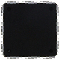
MCF5307AI90B Freescale Semiconductor, MCF5307AI90B Datasheet - Page 246

MCF5307AI90B
Manufacturer Part Number
MCF5307AI90B
Description
IC MPU 32BIT COLDF 90MHZ 208FQFP
Manufacturer
Freescale Semiconductor
Series
MCF530xr
Datasheets
1.MCF5307AI66B.pdf
(484 pages)
2.MCF5307AI66B.pdf
(16 pages)
3.MCF5307AI66B.pdf
(2 pages)
Specifications of MCF5307AI90B
Core Processor
Coldfire V3
Core Size
32-Bit
Speed
90MHz
Connectivity
EBI/EMI, I²C, UART/USART
Peripherals
DMA, POR, WDT
Number Of I /o
16
Program Memory Type
ROMless
Ram Size
4K x 8
Voltage - Supply (vcc/vdd)
3 V ~ 3.6 V
Oscillator Type
External
Operating Temperature
0°C ~ 70°C
Package / Case
208-FQFP
Maximum Clock Frequency
90 MHz
Maximum Operating Temperature
+ 105 C
Mounting Style
SMD/SMT
Minimum Operating Temperature
0 C
Family Name
MCF5xxx
Device Core
ColdFire
Device Core Size
32b
Frequency (max)
90MHz
Instruction Set Architecture
RISC
Supply Voltage 1 (typ)
3.3V
Operating Temp Range
0C to 70C
Operating Temperature Classification
Commercial
Mounting
Surface Mount
Pin Count
208
Package Type
FQFP
Program Memory Size
8KB
Cpu Speed
90MHz
Embedded Interface Type
I2C, UART
Digital Ic Case Style
FQFP
No. Of Pins
208
Supply Voltage Range
3V To 3.6V
Rohs Compliant
Yes
Lead Free Status / RoHS Status
Lead free / RoHS Compliant
Eeprom Size
-
Program Memory Size
-
Data Converters
-
Lead Free Status / Rohs Status
Lead free / RoHS Compliant
Available stocks
Company
Part Number
Manufacturer
Quantity
Price
Company:
Part Number:
MCF5307AI90B
Manufacturer:
FREESCAL
Quantity:
153
Company:
Part Number:
MCF5307AI90B
Manufacturer:
Freescale Semiconductor
Quantity:
10 000
Part Number:
MCF5307AI90B
Manufacturer:
FREESCALE
Quantity:
20 000
- Current page: 246 of 484
- Download datasheet (6Mb)
Asynchronous Operation
Figure 11-6 shows a variation of the basic cycle. In this case, RCD is 1, so there are two
clocks between RAS and CAS. Note that the address is multiplexed on the rising clock
immediately before CAS is asserted. Because RNCN = 0, RAS and CAS are negated
together. The next bus cycle is initiated, but because DACRn[RP] requires RAS to be
precharged for two clocks, RAS is delayed for a clock in the bus cycle. Note that this does
not delay the address signals, only RAS.
11.3.3.2 Burst Page-Mode Operation
Burst page-mode operation (DACRn[PM] = 01) optimizes memory accesses in page mode
by allowing a row address to remain registered in the DRAM while accessing data in
different columns. This eliminates the setup and hold times associated with the need to
precharge and assert RAS. Therefore, only the first bus cycle in the page takes the full
access time; subsequent accesses are streamlined. Single accesses look the same as
non-page-mode accesses.
Burst page-mode accesses of any size—byte, word, longword, or line—are assumed to
reside in the same page. In this mode, the DRAM controller generates a burst transfer only
when the operand is larger than the DRAM block port size (such as, a line transfer to a
32-bit port or a longword transfer to an 8-bit port). The primary cycle asserts RAS and
CAS; subsequent cycles assert only CAS. At the end of the access, RAS is precharged. The
DRAM controller increments addresses between cycles.
Figure 11-7 shows a read access in burst page mode. Four accesses take place, which could
be a 32-bit access to an 8-bit port or a line access to a 32-bit port. Other burst page-mode
operations may be from 2 to 16 accesses long, depending on the access and port sizes. In
those cases, timing is similar with more or fewer accesses.
11-12
RAS[1] or [0]
CAS[3:0]
DRAMW
Figure 11-6. Basic Non-Page-Mode Operation RCD = 1, RNCN = 0 (5-5-5-5)
BCLKO
D[31:0]
A[31:0]
Row
RCD = 1
Freescale Semiconductor, Inc.
For More Information On This Product,
Go to: www.freescale.com
Column
MCF5307 User’s Manual
CAS = 01
RNCN = 0
RP = 01
Related parts for MCF5307AI90B
Image
Part Number
Description
Manufacturer
Datasheet
Request
R
Part Number:
Description:
Manufacturer:
Freescale Semiconductor, Inc
Datasheet:
Part Number:
Description:
Mcf5307 Coldfire Integrated Microprocessor User
Manufacturer:
Freescale Semiconductor, Inc
Datasheet:
Part Number:
Description:
Manufacturer:
Freescale Semiconductor, Inc
Datasheet:
Part Number:
Description:
Manufacturer:
Freescale Semiconductor, Inc
Datasheet:
Part Number:
Description:
Manufacturer:
Freescale Semiconductor, Inc
Datasheet:
Part Number:
Description:
Manufacturer:
Freescale Semiconductor, Inc
Datasheet:
Part Number:
Description:
Manufacturer:
Freescale Semiconductor, Inc
Datasheet:
Part Number:
Description:
Manufacturer:
Freescale Semiconductor, Inc
Datasheet:
Part Number:
Description:
Manufacturer:
Freescale Semiconductor, Inc
Datasheet:
Part Number:
Description:
Manufacturer:
Freescale Semiconductor, Inc
Datasheet:
Part Number:
Description:
Manufacturer:
Freescale Semiconductor, Inc
Datasheet:
Part Number:
Description:
Manufacturer:
Freescale Semiconductor, Inc
Datasheet:
Part Number:
Description:
Manufacturer:
Freescale Semiconductor, Inc
Datasheet:
Part Number:
Description:
Manufacturer:
Freescale Semiconductor, Inc
Datasheet:
Part Number:
Description:
Manufacturer:
Freescale Semiconductor, Inc
Datasheet:


