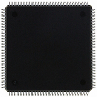
MCF5307AI90B Freescale Semiconductor, MCF5307AI90B Datasheet - Page 395

MCF5307AI90B
Manufacturer Part Number
MCF5307AI90B
Description
IC MPU 32BIT COLDF 90MHZ 208FQFP
Manufacturer
Freescale Semiconductor
Series
MCF530xr
Datasheets
1.MCF5307AI66B.pdf
(484 pages)
2.MCF5307AI66B.pdf
(16 pages)
3.MCF5307AI66B.pdf
(2 pages)
Specifications of MCF5307AI90B
Core Processor
Coldfire V3
Core Size
32-Bit
Speed
90MHz
Connectivity
EBI/EMI, I²C, UART/USART
Peripherals
DMA, POR, WDT
Number Of I /o
16
Program Memory Type
ROMless
Ram Size
4K x 8
Voltage - Supply (vcc/vdd)
3 V ~ 3.6 V
Oscillator Type
External
Operating Temperature
0°C ~ 70°C
Package / Case
208-FQFP
Maximum Clock Frequency
90 MHz
Maximum Operating Temperature
+ 105 C
Mounting Style
SMD/SMT
Minimum Operating Temperature
0 C
Family Name
MCF5xxx
Device Core
ColdFire
Device Core Size
32b
Frequency (max)
90MHz
Instruction Set Architecture
RISC
Supply Voltage 1 (typ)
3.3V
Operating Temp Range
0C to 70C
Operating Temperature Classification
Commercial
Mounting
Surface Mount
Pin Count
208
Package Type
FQFP
Program Memory Size
8KB
Cpu Speed
90MHz
Embedded Interface Type
I2C, UART
Digital Ic Case Style
FQFP
No. Of Pins
208
Supply Voltage Range
3V To 3.6V
Rohs Compliant
Yes
Lead Free Status / RoHS Status
Lead free / RoHS Compliant
Eeprom Size
-
Program Memory Size
-
Data Converters
-
Lead Free Status / Rohs Status
Lead free / RoHS Compliant
Available stocks
Company
Part Number
Manufacturer
Quantity
Price
Company:
Part Number:
MCF5307AI90B
Manufacturer:
FREESCAL
Quantity:
153
Company:
Part Number:
MCF5307AI90B
Manufacturer:
Freescale Semiconductor
Quantity:
10 000
Part Number:
MCF5307AI90B
Manufacturer:
FREESCALE
Quantity:
20 000
- Current page: 395 of 484
- Download datasheet (6Mb)
18.4.3 Read Cycle
During a read cycle, the MCF5307 receives data from memory or from a peripheral device.
Figure 18-5 is a read cycle flowchart.
The read cycle timing diagram is shown in Figure 18-6.
S5
State
S5
Read
Write
1.
2.
3.
4.
5.
6.
1.
1.
Set R/W to read
Place address on A[31:0]
Assert TT[1:0], TM[2:0], TIP,
and SIZ[1:0]
Assert TS
Assert AS
Negate TS
Sample TA low and latch data
Start next cycle
Cycle
An external device has at most two BCLKO cycles after the
start of S4 to three-state the data bus after data is sampled in S3.
This applies to basic read cycles, fast-termination cycles, and
the last transfer of a burst.
In the following timing diagrams, TA waveforms apply for chip
selects programmed to enable either internal or external
termination. TA assertion should look the same in either case.
MCF5307
Low
BCLKO
Table 18-4. Bus Cycle States (Continued)
Freescale Semiconductor, Inc.
For More Information On This Product,
Figure 18-5. Read Cycle Flowchart
AS, CS, BE/BWE, and OE are negated on the BCLKO falling edge. The
MCF5307 stops driving address lines and R/W on the rising edge of BCLKO,
terminating the read or write cycle. At the same time, the MCF5307 negates
TT[1:0], TM[2:0], TIP, and SIZ[1:0] on the rising edge of BCLKO.
Note that the rising edge of BCLKO may be the start of S0 for the next access
cycle; in this case, TIP remains asserted and R/W may not transition,
depending on the nature of the back-to-back cycles.
The external device stops driving data between S4 and S5.
The data bus returns to high impedance on the rising edge of BCLKO. The
rising edge of BCLKO may be the start of S0 for the next access.
Chapter 18. Bus Operation
Go to: www.freescale.com
NOTE:
NOTE:
Description
1.
2.
3.
1.
2.
Decode address and select the
appropriate slave device.
Drive data on D[31:0]
Assert TA
Negate TA.
Stop driving D[31:0]
System
Data Transfer Operation
18-7
Related parts for MCF5307AI90B
Image
Part Number
Description
Manufacturer
Datasheet
Request
R
Part Number:
Description:
Manufacturer:
Freescale Semiconductor, Inc
Datasheet:
Part Number:
Description:
Mcf5307 Coldfire Integrated Microprocessor User
Manufacturer:
Freescale Semiconductor, Inc
Datasheet:
Part Number:
Description:
Manufacturer:
Freescale Semiconductor, Inc
Datasheet:
Part Number:
Description:
Manufacturer:
Freescale Semiconductor, Inc
Datasheet:
Part Number:
Description:
Manufacturer:
Freescale Semiconductor, Inc
Datasheet:
Part Number:
Description:
Manufacturer:
Freescale Semiconductor, Inc
Datasheet:
Part Number:
Description:
Manufacturer:
Freescale Semiconductor, Inc
Datasheet:
Part Number:
Description:
Manufacturer:
Freescale Semiconductor, Inc
Datasheet:
Part Number:
Description:
Manufacturer:
Freescale Semiconductor, Inc
Datasheet:
Part Number:
Description:
Manufacturer:
Freescale Semiconductor, Inc
Datasheet:
Part Number:
Description:
Manufacturer:
Freescale Semiconductor, Inc
Datasheet:
Part Number:
Description:
Manufacturer:
Freescale Semiconductor, Inc
Datasheet:
Part Number:
Description:
Manufacturer:
Freescale Semiconductor, Inc
Datasheet:
Part Number:
Description:
Manufacturer:
Freescale Semiconductor, Inc
Datasheet:
Part Number:
Description:
Manufacturer:
Freescale Semiconductor, Inc
Datasheet:


