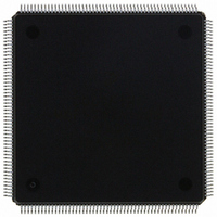
MCF5307AI90B Freescale Semiconductor, MCF5307AI90B Datasheet - Page 64

MCF5307AI90B
Manufacturer Part Number
MCF5307AI90B
Description
IC MPU 32BIT COLDF 90MHZ 208FQFP
Manufacturer
Freescale Semiconductor
Series
MCF530xr
Datasheets
1.MCF5307AI66B.pdf
(484 pages)
2.MCF5307AI66B.pdf
(16 pages)
3.MCF5307AI66B.pdf
(2 pages)
Specifications of MCF5307AI90B
Core Processor
Coldfire V3
Core Size
32-Bit
Speed
90MHz
Connectivity
EBI/EMI, I²C, UART/USART
Peripherals
DMA, POR, WDT
Number Of I /o
16
Program Memory Type
ROMless
Ram Size
4K x 8
Voltage - Supply (vcc/vdd)
3 V ~ 3.6 V
Oscillator Type
External
Operating Temperature
0°C ~ 70°C
Package / Case
208-FQFP
Maximum Clock Frequency
90 MHz
Maximum Operating Temperature
+ 105 C
Mounting Style
SMD/SMT
Minimum Operating Temperature
0 C
Family Name
MCF5xxx
Device Core
ColdFire
Device Core Size
32b
Frequency (max)
90MHz
Instruction Set Architecture
RISC
Supply Voltage 1 (typ)
3.3V
Operating Temp Range
0C to 70C
Operating Temperature Classification
Commercial
Mounting
Surface Mount
Pin Count
208
Package Type
FQFP
Program Memory Size
8KB
Cpu Speed
90MHz
Embedded Interface Type
I2C, UART
Digital Ic Case Style
FQFP
No. Of Pins
208
Supply Voltage Range
3V To 3.6V
Rohs Compliant
Yes
Lead Free Status / RoHS Status
Lead free / RoHS Compliant
Eeprom Size
-
Program Memory Size
-
Data Converters
-
Lead Free Status / Rohs Status
Lead free / RoHS Compliant
Available stocks
Company
Part Number
Manufacturer
Quantity
Price
Company:
Part Number:
MCF5307AI90B
Manufacturer:
FREESCAL
Quantity:
153
Company:
Part Number:
MCF5307AI90B
Manufacturer:
Freescale Semiconductor
Quantity:
10 000
Part Number:
MCF5307AI90B
Manufacturer:
FREESCALE
Quantity:
20 000
- Current page: 64 of 484
- Download datasheet (6Mb)
Features and Enhancements
For example, if an unconditional BRA instruction is detected, the IED calculates the target
of the BRA instruction, and the IAG immediately begins fetching at the target address.
Because of the decoupled nature of the two pipelines, the target instruction is available to
the OEP immediately after the BRA instruction, giving it a single-cycle execution time.
The acceleration logic uses a static prediction algorithm when processing conditional
branch (Bcc) instructions. The default scheme is forward Bcc instructions are predicted as
not-taken, while backward Bcc instructions are predicted as taken. A user-mode control bit,
CCR[7], allows users to dynamically alter the prediction algorithm for forward Bcc
instructions. See Section 2.2.1.5, “Condition Code Register (CCR).
2.1.2.2 Operand Execution Pipeline (OEP)
The OEP is a two-stage pipeline featuring a traditional RISC datapath with a register file
feeding an arithmetic/logic unit. For simple register-to-register instructions, the first stage
of the OEP performs the instruction decode and fetching of the required register operands
(OC), while the actual instruction execution is performed in the second stage (EX).
For memory-to-register instructions, the instruction is effectively staged through the OEP
twice in the following way:
For register-to-memory operations, the stage functions (DS/OC, AG/EX) are effectively
performed simultaneously allowing single-cycle execution. For read-modify-write
instructions, the pipeline effectively combines a memory-to-register operation with a store
operation.
2.1.2.2.1 Illegal Opcode Handling
To aid in conversion from M68000 code, every 16-bit operation word is decoded to ensure
that each instruction is valid. If the processor attempts execution of an illegal or
unsupported instruction, an illegal instruction exception (vector 4) is taken.
2.1.2.2.2 Hardware Multiply/Accumulate (MAC) Unit
The MAC is an optional unit in Version 3 that provides hardware support for a limited set
of digital signal processing (DSP) operations used in embedded code, while supporting the
integer multiply instructions in the ColdFire microprocessor family. The MAC features a
three-stage execution pipeline, optimized for 16 x 16 multiplies. It is tightly coupled to the
OEP, which can issue a 16 x 16 multiply with a 32-bit accumulation plus fetch a 32-bit
operand in a single cycle. A 32 x 32 multiply with a 32-bit accumulation requires three
cycles before the next instruction can be issued.
2-24
• The instruction is decoded and the components of the operand address are selected
• The operand address is generated using the “execute engine” (AG).
• The memory operand is fetched while any register operand is simultaneously
• The instruction is executed (EX).
(DS).
fetched (OC).
Freescale Semiconductor, Inc.
For More Information On This Product,
Go to: www.freescale.com
MCF5307 User’s Manual
Related parts for MCF5307AI90B
Image
Part Number
Description
Manufacturer
Datasheet
Request
R
Part Number:
Description:
Manufacturer:
Freescale Semiconductor, Inc
Datasheet:
Part Number:
Description:
Mcf5307 Coldfire Integrated Microprocessor User
Manufacturer:
Freescale Semiconductor, Inc
Datasheet:
Part Number:
Description:
Manufacturer:
Freescale Semiconductor, Inc
Datasheet:
Part Number:
Description:
Manufacturer:
Freescale Semiconductor, Inc
Datasheet:
Part Number:
Description:
Manufacturer:
Freescale Semiconductor, Inc
Datasheet:
Part Number:
Description:
Manufacturer:
Freescale Semiconductor, Inc
Datasheet:
Part Number:
Description:
Manufacturer:
Freescale Semiconductor, Inc
Datasheet:
Part Number:
Description:
Manufacturer:
Freescale Semiconductor, Inc
Datasheet:
Part Number:
Description:
Manufacturer:
Freescale Semiconductor, Inc
Datasheet:
Part Number:
Description:
Manufacturer:
Freescale Semiconductor, Inc
Datasheet:
Part Number:
Description:
Manufacturer:
Freescale Semiconductor, Inc
Datasheet:
Part Number:
Description:
Manufacturer:
Freescale Semiconductor, Inc
Datasheet:
Part Number:
Description:
Manufacturer:
Freescale Semiconductor, Inc
Datasheet:
Part Number:
Description:
Manufacturer:
Freescale Semiconductor, Inc
Datasheet:
Part Number:
Description:
Manufacturer:
Freescale Semiconductor, Inc
Datasheet:


