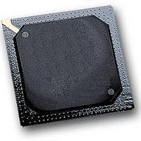
MPC564CVR40 Freescale Semiconductor, MPC564CVR40 Datasheet - Page 127

MPC564CVR40
Manufacturer Part Number
MPC564CVR40
Description
IC MPU 32BIT W/CODE COMP 388PBGA
Manufacturer
Freescale Semiconductor
Series
MPC5xxr
Specifications of MPC564CVR40
Core Processor
PowerPC
Core Size
32-Bit
Speed
40MHz
Connectivity
CAN, EBI/EMI, SCI, SPI, UART/USART
Peripherals
POR, PWM, WDT
Number Of I /o
56
Program Memory Size
512KB (512K x 8)
Program Memory Type
FLASH
Ram Size
32K x 8
Voltage - Supply (vcc/vdd)
2.5 V ~ 2.7 V
Data Converters
A/D 32x10b
Oscillator Type
External
Operating Temperature
-40°C ~ 85°C
Package / Case
388-BGA
Processor Series
MPC5xx
Core
PowerPC
Data Bus Width
32 bit
Data Ram Size
32 KB
Interface Type
CAN, JTAG, QSPI, SCI, SPI, UART
Maximum Clock Frequency
40 MHz
Number Of Programmable I/os
56
Number Of Timers
2
Maximum Operating Temperature
+ 85 C
Mounting Style
SMD/SMT
Minimum Operating Temperature
- 40 C
On-chip Adc
2 (10 bit, 32 Channel)
For Use With
MPC564EVB - KIT EVAL FOR MPC561/562/563/564
Lead Free Status / RoHS Status
Lead free / RoHS Compliant
Eeprom Size
-
Lead Free Status / Rohs Status
Details
Available stocks
Company
Part Number
Manufacturer
Quantity
Price
Company:
Part Number:
MPC564CVR40
Manufacturer:
Freescale Semiconductor
Quantity:
10 000
- Current page: 127 of 1420
- Download datasheet (11Mb)
2.5.1
The MPC561/MPC563 has five JTAG signals. The test data input (TDI) and test data output (TDO) scan
ports are used to scan instructions as well as data into the various scan registers for JTAG operations. The
scan operation is controlled by the test access port (TAP) controller, which in turn is controlled by the test
mode select (TMS) input sequence. The scan data is latched at the rising edge of the test clock (TCK).
On the MPC561/MPC563, JTAG is used for boundary scan only. There is no access to internal
MPC561/MPC563 circuitry. When JTAG mode is enabled, the READI module will be held inactive. See
Figure 2-4
JTAG is entered by the following sequence of events:
JTAG mode is exited by:
Freescale Semiconductor
•
•
•
Assert PORESET/TRST to reset the JTAG TAP controller
Hold JCOMP/RSTI high prior to PORESET/TRST negation and keep high as long as JTAG mode
is required
(The READI module will be held inactive since only one of the multiplexed functions JCOMP and
RSTI can be asserted at the negation of PORESET/TRST).
Drive JCOMP/RSTI low.
for JTAG mode selection.
JTAG Mode Selection
JCOMP
Signal
DSCK
DSDI
MDI0
EVTI
PORESET/TRST and analog signals ANx, EXTAL, XTAL, and
TDI/TDO/TMS/TCK are not in the JTAG scan path.
Table 2-13. MPC561/MPC563 Mode Selection Options
MPC561/MPC563 Reference Manual, Rev. 1.2
State
High
High
High
High
High
Low
Low
Low
Low
Low
Nexus Configuration
JTAG Selection
BDM Mode
NOTE
8 clocks after SRESET
8 clocks after SRESET
SRESET negation
SRESET negation
When Sampled
RSTI negation
RSTI negation
EVTI negation
EVTI negation
PORESET
PORESET
READI module Disabled
READI module Enabled
Nexus or BDM allowed
JTAG Mode Selected
Asynchronous mode
BDM mode disabled
BDM mode enabled
Reduced port mode
Synchronous mode
Full Port mode
Affect
Signal Descriptions
2-29
Related parts for MPC564CVR40
Image
Part Number
Description
Manufacturer
Datasheet
Request
R

Part Number:
Description:
MPC5 1K0 5%
Manufacturer:
TE Connectivity
Datasheet:

Part Number:
Description:
MPC5 500R 5%
Manufacturer:
TE Connectivity
Datasheet:

Part Number:
Description:
MPC5 5K0 5%
Manufacturer:
Tyco Electronics
Datasheet:

Part Number:
Description:
MPC5 5R0 5%
Manufacturer:
Tyco Electronics
Datasheet:

Part Number:
Description:
MPC5 50K 5%
Manufacturer:
Tyco Electronics
Datasheet:

Part Number:
Description:
MPC5 1R0 5%
Manufacturer:
Tyco Electronics
Datasheet:
Part Number:
Description:
Manufacturer:
Freescale Semiconductor, Inc
Datasheet:
Part Number:
Description:
Manufacturer:
Freescale Semiconductor, Inc
Datasheet:
Part Number:
Description:
Manufacturer:
Freescale Semiconductor, Inc
Datasheet:
Part Number:
Description:
Manufacturer:
Freescale Semiconductor, Inc
Datasheet:
Part Number:
Description:
Manufacturer:
Freescale Semiconductor, Inc
Datasheet:


