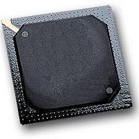
MPC564CVR40 Freescale Semiconductor, MPC564CVR40 Datasheet - Page 1312

MPC564CVR40
Manufacturer Part Number
MPC564CVR40
Description
IC MPU 32BIT W/CODE COMP 388PBGA
Manufacturer
Freescale Semiconductor
Series
MPC5xxr
Specifications of MPC564CVR40
Core Processor
PowerPC
Core Size
32-Bit
Speed
40MHz
Connectivity
CAN, EBI/EMI, SCI, SPI, UART/USART
Peripherals
POR, PWM, WDT
Number Of I /o
56
Program Memory Size
512KB (512K x 8)
Program Memory Type
FLASH
Ram Size
32K x 8
Voltage - Supply (vcc/vdd)
2.5 V ~ 2.7 V
Data Converters
A/D 32x10b
Oscillator Type
External
Operating Temperature
-40°C ~ 85°C
Package / Case
388-BGA
Processor Series
MPC5xx
Core
PowerPC
Data Bus Width
32 bit
Data Ram Size
32 KB
Interface Type
CAN, JTAG, QSPI, SCI, SPI, UART
Maximum Clock Frequency
40 MHz
Number Of Programmable I/os
56
Number Of Timers
2
Maximum Operating Temperature
+ 85 C
Mounting Style
SMD/SMT
Minimum Operating Temperature
- 40 C
On-chip Adc
2 (10 bit, 32 Channel)
For Use With
MPC564EVB - KIT EVAL FOR MPC561/562/563/564
Lead Free Status / RoHS Status
Lead free / RoHS Compliant
Eeprom Size
-
Lead Free Status / Rohs Status
Details
Available stocks
Company
Part Number
Manufacturer
Quantity
Price
Company:
Part Number:
MPC564CVR40
Manufacturer:
Freescale Semiconductor
Quantity:
10 000
- Current page: 1312 of 1420
- Download datasheet (11Mb)
66-MHz Electrical Characteristics
should be positioned so that the thermocouple junction rests on the package. A small amount of epoxy is
placed over the thermocouple junction and over about one mm of wire extending from the junction. The
thermocouple wire is placed flat against the package case to avoid measurement errors caused by cooling
effects of the thermocouple wire.
G.4.1
The website for Semiconductor Equipment and Materials International is www.semi.org and their global
headquarters address is: 3081 Zanker Road, San Jose CA, 95134; 1-408-943-6900.
MIL-SPEC and EIA/JESD (JEDEC) specifications are available from Global Engineering Documents on
the WEB at www.global.ihs.com or 800-854-7179 or 303-397-7956.
JEDEC specifications are available on the WEB at www.jedec.org.
G.5
G-6
1. C.E. Triplett and B. Joiner, “An Experimental Characterization of a 272 PBGA Within an
2. B. Joiner and V. Adams, “Measurement and Simulation of Junction to Board Thermal Resistance
1
2
ESD for Human Body Model (HBM)
HBM Circuit Description
ESD for Machine Model (MM)
MM Circuit Description
Number of pulses per pin
Positive pulses (MM)
Negative pulses (MM)
Positive pulses (HBM)
Negative pulses (HBM)
Interval of Pulses
Automotive Engine Controller Module,” Proceedings of SemiTherm, San Diego, 1998, pp. 47-54.
and Its Application in Thermal Modeling,” Proceedings of SemiTherm, San Diego, 1999, pp.
212-220.
All ESD testing is in conformity with CDF-AEC-Q100 Stress Test Qualification for Automotive Grade Integrated
Circuits.
A device will be defined as a failure if after exposure to ESD pulses the device no longer meets the device
specification requirements. Complete DC parametric and functional testing shall be performed per applicable
device specification at room temperature followed by hot temperature, unless specified otherwise in the device
specification.
ESD Protection
Thermal References
Characteristics
2
MPC561/MPC563 Reference Manual, Rev. 1.2
1
Table G-3. ESD Protection
Symbol
R1
R1
—
—
—
—
—
C
C
Value
2000
1500
100
200
200
0
3
3
1
1
1
Freescale Semiconductor
Units
pF
pF
—
Ω
Ω
S
V
V
Related parts for MPC564CVR40
Image
Part Number
Description
Manufacturer
Datasheet
Request
R

Part Number:
Description:
MPC5 1K0 5%
Manufacturer:
TE Connectivity
Datasheet:

Part Number:
Description:
MPC5 500R 5%
Manufacturer:
TE Connectivity
Datasheet:

Part Number:
Description:
MPC5 5K0 5%
Manufacturer:
Tyco Electronics
Datasheet:

Part Number:
Description:
MPC5 5R0 5%
Manufacturer:
Tyco Electronics
Datasheet:

Part Number:
Description:
MPC5 50K 5%
Manufacturer:
Tyco Electronics
Datasheet:

Part Number:
Description:
MPC5 1R0 5%
Manufacturer:
Tyco Electronics
Datasheet:
Part Number:
Description:
Manufacturer:
Freescale Semiconductor, Inc
Datasheet:
Part Number:
Description:
Manufacturer:
Freescale Semiconductor, Inc
Datasheet:
Part Number:
Description:
Manufacturer:
Freescale Semiconductor, Inc
Datasheet:
Part Number:
Description:
Manufacturer:
Freescale Semiconductor, Inc
Datasheet:
Part Number:
Description:
Manufacturer:
Freescale Semiconductor, Inc
Datasheet:


