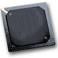
MPC564CVR40 Freescale Semiconductor, MPC564CVR40 Datasheet - Page 355

MPC564CVR40
Manufacturer Part Number
MPC564CVR40
Description
IC MPU 32BIT W/CODE COMP 388PBGA
Manufacturer
Freescale Semiconductor
Series
MPC5xxr
Specifications of MPC564CVR40
Core Processor
PowerPC
Core Size
32-Bit
Speed
40MHz
Connectivity
CAN, EBI/EMI, SCI, SPI, UART/USART
Peripherals
POR, PWM, WDT
Number Of I /o
56
Program Memory Size
512KB (512K x 8)
Program Memory Type
FLASH
Ram Size
32K x 8
Voltage - Supply (vcc/vdd)
2.5 V ~ 2.7 V
Data Converters
A/D 32x10b
Oscillator Type
External
Operating Temperature
-40°C ~ 85°C
Package / Case
388-BGA
Processor Series
MPC5xx
Core
PowerPC
Data Bus Width
32 bit
Data Ram Size
32 KB
Interface Type
CAN, JTAG, QSPI, SCI, SPI, UART
Maximum Clock Frequency
40 MHz
Number Of Programmable I/os
56
Number Of Timers
2
Maximum Operating Temperature
+ 85 C
Mounting Style
SMD/SMT
Minimum Operating Temperature
- 40 C
On-chip Adc
2 (10 bit, 32 Channel)
For Use With
MPC564EVB - KIT EVAL FOR MPC561/562/563/564
Lead Free Status / RoHS Status
Lead free / RoHS Compliant
Eeprom Size
-
Lead Free Status / Rohs Status
Details
Available stocks
Company
Part Number
Manufacturer
Quantity
Price
Company:
Part Number:
MPC564CVR40
Manufacturer:
Freescale Semiconductor
Quantity:
10 000
- Current page: 355 of 1420
- Download datasheet (11Mb)
1. For an illustration of device connections on the data bus, see
9.5.3
Pre-discharge mode is provided for applications that use 3.3-V/5-V external memories while the
MPC561/MPC563 data bus pads are optimized to 2.6-V memories, and cannot tolerate more than 3.1 V.
When connecting 3.3-V devices to the E-bus, and performing read and write operations, this mode should
be invoked in order to avoid long term reliability issues of the data pads.
When the PDMCR2[PREDIS_EN] bit is set, the MPC561/MPC563 will discharge the bus during the
address phase of any write cycle prior to the data phase. The data bus will be discharged from up to 5 V to
a level which is suitable to the low voltage drivers. In most cases, the ORx[EHTR] bit of the relevant
memory bank, should be set along with the PREDIS_EN bit in order to reserve sufficient time for the
Freescale Semiconductor
CLKOUT
BR
BG
BB
ADDR[0:1]
RD/WR
TSIZ[0:1]
BURST, BDIP
TS
STS
Data
TA
1
Data Bus Pre-Discharge Mode
Figure 9-10. Single Beat 32-Bit Data Write Cycle Timing — 16-Bit Port Size
MPC561/MPC563 Reference Manual, Rev. 1.2
ADDR
00
ABCDEFGH
Figure
9-23.
10
ADDR + 2
EFGHEFGH
External Bus Interface
9-15
Related parts for MPC564CVR40
Image
Part Number
Description
Manufacturer
Datasheet
Request
R

Part Number:
Description:
MPC5 1K0 5%
Manufacturer:
TE Connectivity
Datasheet:

Part Number:
Description:
MPC5 500R 5%
Manufacturer:
TE Connectivity
Datasheet:

Part Number:
Description:
MPC5 5K0 5%
Manufacturer:
Tyco Electronics
Datasheet:

Part Number:
Description:
MPC5 5R0 5%
Manufacturer:
Tyco Electronics
Datasheet:

Part Number:
Description:
MPC5 50K 5%
Manufacturer:
Tyco Electronics
Datasheet:

Part Number:
Description:
MPC5 1R0 5%
Manufacturer:
Tyco Electronics
Datasheet:
Part Number:
Description:
Manufacturer:
Freescale Semiconductor, Inc
Datasheet:
Part Number:
Description:
Manufacturer:
Freescale Semiconductor, Inc
Datasheet:
Part Number:
Description:
Manufacturer:
Freescale Semiconductor, Inc
Datasheet:
Part Number:
Description:
Manufacturer:
Freescale Semiconductor, Inc
Datasheet:
Part Number:
Description:
Manufacturer:
Freescale Semiconductor, Inc
Datasheet:


