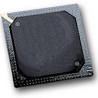
MPC564CVR40 Freescale Semiconductor, MPC564CVR40 Datasheet - Page 517

MPC564CVR40
Manufacturer Part Number
MPC564CVR40
Description
IC MPU 32BIT W/CODE COMP 388PBGA
Manufacturer
Freescale Semiconductor
Series
MPC5xxr
Specifications of MPC564CVR40
Core Processor
PowerPC
Core Size
32-Bit
Speed
40MHz
Connectivity
CAN, EBI/EMI, SCI, SPI, UART/USART
Peripherals
POR, PWM, WDT
Number Of I /o
56
Program Memory Size
512KB (512K x 8)
Program Memory Type
FLASH
Ram Size
32K x 8
Voltage - Supply (vcc/vdd)
2.5 V ~ 2.7 V
Data Converters
A/D 32x10b
Oscillator Type
External
Operating Temperature
-40°C ~ 85°C
Package / Case
388-BGA
Processor Series
MPC5xx
Core
PowerPC
Data Bus Width
32 bit
Data Ram Size
32 KB
Interface Type
CAN, JTAG, QSPI, SCI, SPI, UART
Maximum Clock Frequency
40 MHz
Number Of Programmable I/os
56
Number Of Timers
2
Maximum Operating Temperature
+ 85 C
Mounting Style
SMD/SMT
Minimum Operating Temperature
- 40 C
On-chip Adc
2 (10 bit, 32 Channel)
For Use With
MPC564EVB - KIT EVAL FOR MPC561/562/563/564
Lead Free Status / RoHS Status
Lead free / RoHS Compliant
Eeprom Size
-
Lead Free Status / Rohs Status
Details
Available stocks
Company
Part Number
Manufacturer
Quantity
Price
Company:
Part Number:
MPC564CVR40
Manufacturer:
Freescale Semiconductor
Quantity:
10 000
- Current page: 517 of 1420
- Download datasheet (11Mb)
Byte access to an even address of a QADC64E location is shown in the top illustration of
the case of write cycles, byte 1 of the register is not disturbed. In the case of a read cycle, the QADC64E
provides both byte 0 and byte 1.
Byte access to an odd address of a QADC64E location is shown in the center illustration of
In the case of write cycles, byte 0 of the register is not disturbed. In the case of read cycles, the QADC64E
provides both byte 0 and byte 1.
16-bit accesses to an even address read or write byte 0 and byte 1 as shown in the lowest illustration of
Figure
16-bit accesses to an odd address require two bus cycles; one byte of two different 16-bit QADC64E
locations is accessed. The first bus cycle is treated by the QADC64E as an 8-bit read or write of an odd
address. The second cycle is an 8-bit read or write of an even address. The QADC64E address space is
organized into 16-bit even address locations, so a 16-bit read or write of an odd address obtains or provides
the lower half of one QADC64E location, and the upper half of the following QADC64E location.
Freescale Semiconductor
13-26. The full 16 bits of data is written to and read from the QADC64E location with each access.
Intermodule Bus
Intermodule Bus
Intermodule Bus
QADC Location
QADC Location
QADC Location
8-bit Access of an Odd Address (ISIZ = 01, A0 = 1; OR ISIZ = 10, A0 = 1)
MPC561/MPC563 Reference Manual, Rev. 1.2
Figure 13-26. Bus Cycle Accesses
8-bit Access of an Even Address (ISIZ = 01, A0 = 0)
W
W
W
16-Bit Aligned Access (ISIZ = 10, A0 = 0)
Byte 0
Byte 0
Byte 0
Byte 0
BYTE 0
BYTE 0
R
R
R
W
W
W
Byte 1
Byte 1
Byte 1
Byte 1
BYTE 1
BYTE 1
R
R
R
QADC64E Legacy Mode Operation
QADC64E Bus CYC ACC
Figure
Figure
13-26. In
13-26.
13-53
Related parts for MPC564CVR40
Image
Part Number
Description
Manufacturer
Datasheet
Request
R

Part Number:
Description:
MPC5 1K0 5%
Manufacturer:
TE Connectivity
Datasheet:

Part Number:
Description:
MPC5 500R 5%
Manufacturer:
TE Connectivity
Datasheet:

Part Number:
Description:
MPC5 5K0 5%
Manufacturer:
Tyco Electronics
Datasheet:

Part Number:
Description:
MPC5 5R0 5%
Manufacturer:
Tyco Electronics
Datasheet:

Part Number:
Description:
MPC5 50K 5%
Manufacturer:
Tyco Electronics
Datasheet:

Part Number:
Description:
MPC5 1R0 5%
Manufacturer:
Tyco Electronics
Datasheet:
Part Number:
Description:
Manufacturer:
Freescale Semiconductor, Inc
Datasheet:
Part Number:
Description:
Manufacturer:
Freescale Semiconductor, Inc
Datasheet:
Part Number:
Description:
Manufacturer:
Freescale Semiconductor, Inc
Datasheet:
Part Number:
Description:
Manufacturer:
Freescale Semiconductor, Inc
Datasheet:
Part Number:
Description:
Manufacturer:
Freescale Semiconductor, Inc
Datasheet:


