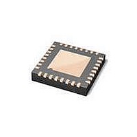
LPC1113FHN33/302,5 NXP Semiconductors, LPC1113FHN33/302,5 Datasheet - Page 16

LPC1113FHN33/302,5
Manufacturer Part Number
LPC1113FHN33/302,5
Description
IC MCU LV 32BIT 24K FLAS 32VQFN
Manufacturer
NXP Semiconductors
Series
LPC1100Lr
Datasheet
1.LPC1114FHN333015.pdf
(66 pages)
Specifications of LPC1113FHN33/302,5
Featured Product
LPC1100L 32-Bit MCU
Core Processor
ARM Cortex-M0
Core Size
32-Bit
Speed
50MHz
Connectivity
I²C, SPI, UART/USART
Peripherals
Brown-out Detect/Reset, POR, WDT
Number Of I /o
28
Program Memory Size
24KB (24K x 8)
Program Memory Type
FLASH
Ram Size
8K x 8
Voltage - Supply (vcc/vdd)
1.8 V ~ 3.6 V
Data Converters
A/D 8x10b
Oscillator Type
Internal
Operating Temperature
-40°C ~ 85°C
Package / Case
32-VQFN Exposed Pad
Processor Series
LPC1113
Core
ARM Cortex-M0
Data Bus Width
32 bit
Data Ram Size
8 KB
Interface Type
I2C, UART, SPI, SSP
Maximum Clock Frequency
50 MHz
Number Of Programmable I/os
42
Number Of Timers
4
Maximum Operating Temperature
+ 85 C
Mounting Style
SMD/SMT
Lead Free Status / RoHS Status
Lead free / RoHS Compliant
Eeprom Size
-
Lead Free Status / Rohs Status
Details
Other names
568-5148
NXP Semiconductors
Table 4.
[1]
[2]
[3]
[4]
[5]
[6]
Table 5.
LPC1111_12_13_14
Product data sheet
Symbol
PIO3_5
V
XTALIN
XTALOUT
V
Symbol
PIO0_0 to PIO0_11
RESET/PIO0_0
PIO0_1/CLKOUT/
CT32B0_MAT2
PIO0_2/SSEL0/
CT16B0_CAP0
PIO0_3
PIO0_4/SCL
DD
SS
Pin state at reset for default function: I = Input; O = Output; PU = internal pull-up enabled; IA = inactive, no pull-up/down enabled.
See
reset the chip and wake up from Deep power-down mode. An external pull-up resistor is required on this pin for the Deep power-down
mode.
5 V tolerant pad providing digital I/O functions with configurable pull-up/pull-down resistors and configurable hysteresis (see
I
5 V tolerant pad providing digital I/O functions with configurable pull-up/pull-down resistors, configurable hysteresis, and analog input.
When configured as a ADC input, digital section of the pad is disabled and the pin is not 5 V tolerant (see
When the system oscillator is not used, connect XTALIN and XTALOUT as follows: XTALIN can be left floating or can be grounded
(grounding is preferred to reduce susceptibility to noise). XTALOUT should be left floating.
2
C-bus pads compliant with the I
Figure 33
LPC1114 pin description table (PLCC44 package)
LPC1111/12/13/14 pin description table (HVQFN33 package)
for the reset pad configuration. RESET functionality is not available in Deep power-down mode. Use the WAKEUP pin to
Pin
2
3
8
9
10
[2]
[3]
[3]
[3]
Pin
25
1; 12 -
10
11
9; 43 -
[4]
[6]
[3]
[6]
Start
logic
input
yes
yes
yes
yes
yes
Start
logic
input
no
-
-
2
C-bus specification for I
Type Reset
I
I/O
I/O
O
O
I/O
I/O
I
I/O
I/O
I/O
Type Reset
I/O
I
I
O
I
All information provided in this document is subject to legal disclaimers.
state
[1]
I;PU
-
I;PU
-
-
I;PU
-
-
I;PU
I;PU
-
state
[1]
I; PU
-
-
-
-
Rev. 4 — 10 February 2011
Description
Port 0 — Port 0 is a 12-bit I/O port with individual direction and
function controls for each bit. The operation of port 0 pins depends on
the function selected through the IOCONFIG register block.
RESET — External reset input with 20 ns glitch filter. A LOW-going
pulse as short as 50 ns on this pin resets the device, causing I/O ports
and peripherals to take on their default states and processor execution
to begin at address 0.
PIO0_0 — General purpose digital input/output pin with 10 ns glitch
filter.
PIO0_1 — General purpose digital input/output pin. A LOW level on
this pin during reset starts the ISP command handler.
CLKOUT — Clock out pin.
CT32B0_MAT2 — Match output 2 for 32-bit timer 0.
PIO0_2 — General purpose digital input/output pin.
SSEL0 — Slave select for SPI0.
CT16B0_CAP0 — Capture input 0 for 16-bit timer 0.
PIO0_3 — General purpose digital input/output pin.
PIO0_4 — General purpose digital input/output pin (open-drain).
SCL — I
if I
Description
PIO3_5 — General purpose digital input/output pin.
3.3 V supply voltage to the internal regulator, the external rail, and
the ADC. Also used as the ADC reference voltage.
Input to the oscillator circuit and internal clock generator circuits.
Input voltage must not exceed 1.8 V.
Output from the oscillator amplifier.
Ground.
2
2
C standard mode and I
C Fast-mode Plus is selected in the I/O configuration register.
2
C-bus, open-drain clock input/output. High-current sink only
…continued
2
C Fast-mode Plus.
32-bit ARM Cortex-M0 microcontroller
LPC1111/12/13/14
Figure
© NXP B.V. 2011. All rights reserved.
32).
Figure
16 of 66
32).


