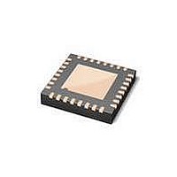
LPC1113FHN33/302,5 NXP Semiconductors, LPC1113FHN33/302,5 Datasheet - Page 24

LPC1113FHN33/302,5
Manufacturer Part Number
LPC1113FHN33/302,5
Description
IC MCU LV 32BIT 24K FLAS 32VQFN
Manufacturer
NXP Semiconductors
Series
LPC1100Lr
Datasheet
1.LPC1114FHN333015.pdf
(66 pages)
Specifications of LPC1113FHN33/302,5
Featured Product
LPC1100L 32-Bit MCU
Core Processor
ARM Cortex-M0
Core Size
32-Bit
Speed
50MHz
Connectivity
I²C, SPI, UART/USART
Peripherals
Brown-out Detect/Reset, POR, WDT
Number Of I /o
28
Program Memory Size
24KB (24K x 8)
Program Memory Type
FLASH
Ram Size
8K x 8
Voltage - Supply (vcc/vdd)
1.8 V ~ 3.6 V
Data Converters
A/D 8x10b
Oscillator Type
Internal
Operating Temperature
-40°C ~ 85°C
Package / Case
32-VQFN Exposed Pad
Processor Series
LPC1113
Core
ARM Cortex-M0
Data Bus Width
32 bit
Data Ram Size
8 KB
Interface Type
I2C, UART, SPI, SSP
Maximum Clock Frequency
50 MHz
Number Of Programmable I/os
42
Number Of Timers
4
Maximum Operating Temperature
+ 85 C
Mounting Style
SMD/SMT
Lead Free Status / RoHS Status
Lead free / RoHS Compliant
Eeprom Size
-
Lead Free Status / Rohs Status
Details
Other names
568-5148
NXP Semiconductors
LPC1111_12_13_14
Product data sheet
7.10.1 Features
7.12.1 Features
7.11.1 Features
7.12 General purpose external event counter/timers
7.11 10-bit ADC
receivers can operate in either master or slave mode, depending on whether the chip has
to initiate a data transfer or is only addressed. The I
controlled by more than one bus master connected to it.
The LPC1111/12/13/14 contains one ADC. It is a single 10-bit successive approximation
ADC with eight channels.
The LPC1111/12/13/14 includes two 32-bit counter/timers and two 16-bit counter/timers.
The counter/timer is designed to count cycles of the system derived clock. It can optionally
generate interrupts or perform other actions at specified timer values, based on four
match registers. Each counter/timer also includes one capture input to trap the timer value
when an input signal transitions, optionally generating an interrupt.
•
•
•
•
•
•
•
•
•
•
•
•
•
•
•
•
•
•
•
The I
I
Easy to configure as master, slave, or master/slave.
Programmable clocks allow versatile rate control.
Bidirectional data transfer between masters and slaves.
Multi-master bus (no central master).
Arbitration between simultaneously transmitting masters without corruption of serial
data on the bus.
Serial clock synchronization allows devices with different bit rates to communicate via
one serial bus.
Serial clock synchronization can be used as a handshake mechanism to suspend and
resume serial transfer.
The I
The I
10-bit successive approximation ADC.
Input multiplexing among 8 pins.
Power-down mode.
Measurement range 0 V to V
10-bit conversion time ≥ 2.44 μs.
Burst conversion mode for single or multiple inputs.
Optional conversion on transition of input pin or timer match signal.
Individual result registers for each ADC channel to reduce interrupt overhead.
A 32-bit/16-bit timer/counter with a programmable 32-bit/16-bit prescaler.
2
C-bus interface also supports Fast-mode Plus with bit rates up to 1 Mbit/s.
2
2
2
C-interface is a standard I
C-bus can be used for test and diagnostic purposes.
C-bus controller supports multiple address recognition and a bus monitor mode.
All information provided in this document is subject to legal disclaimers.
Rev. 4 — 10 February 2011
DD
.
2
C-bus compliant interface with open-drain pins. The
32-bit ARM Cortex-M0 microcontroller
2
LPC1111/12/13/14
C is a multi-master bus and can be
© NXP B.V. 2011. All rights reserved.
24 of 66


