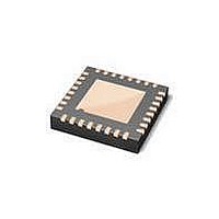
LPC1113FHN33/302,5 NXP Semiconductors, LPC1113FHN33/302,5 Datasheet - Page 63

LPC1113FHN33/302,5
Manufacturer Part Number
LPC1113FHN33/302,5
Description
IC MCU LV 32BIT 24K FLAS 32VQFN
Manufacturer
NXP Semiconductors
Series
LPC1100Lr
Datasheet
1.LPC1114FHN333015.pdf
(66 pages)
Specifications of LPC1113FHN33/302,5
Featured Product
LPC1100L 32-Bit MCU
Core Processor
ARM Cortex-M0
Core Size
32-Bit
Speed
50MHz
Connectivity
I²C, SPI, UART/USART
Peripherals
Brown-out Detect/Reset, POR, WDT
Number Of I /o
28
Program Memory Size
24KB (24K x 8)
Program Memory Type
FLASH
Ram Size
8K x 8
Voltage - Supply (vcc/vdd)
1.8 V ~ 3.6 V
Data Converters
A/D 8x10b
Oscillator Type
Internal
Operating Temperature
-40°C ~ 85°C
Package / Case
32-VQFN Exposed Pad
Processor Series
LPC1113
Core
ARM Cortex-M0
Data Bus Width
32 bit
Data Ram Size
8 KB
Interface Type
I2C, UART, SPI, SSP
Maximum Clock Frequency
50 MHz
Number Of Programmable I/os
42
Number Of Timers
4
Maximum Operating Temperature
+ 85 C
Mounting Style
SMD/SMT
Lead Free Status / RoHS Status
Lead free / RoHS Compliant
Eeprom Size
-
Lead Free Status / Rohs Status
Details
Other names
568-5148
NXP Semiconductors
14. Revision history
Table 23.
LPC1111_12_13_14
Product data sheet
Document ID
LPC1111_12_13_14 v.4
Modifications:
LPC1111_12_13_14 v.3
Modifications:
LPC1111_12_13_14 v.2
Modifications:
LPC1111_12_13_14 v.1
Revision history
Release date
20110210
20101110
20100818
20100416
•
•
•
•
•
•
•
•
•
•
•
•
•
•
•
•
•
•
•
•
•
Power consumption graphs added for parts LPC111x/102/202/302
Figure
Parameter V
Typical value for parameter N
I
(minimum) for 2.0 V ≤ V
Section 11.6 “ElectroMagnetic Compatibility (EMC)”
Power-up characterization added
Parts LPC111x/102/202/302 added (LPC1100L series).
Power consumption data for parts LPC111x/102/202/302 added in Table 7.
PLL output frequency limited to 100 MHz in Section 7.15.2.
Description of RESET and WAKEUP functions updated in Section 6.
WDT description updated in Section 7.14. The WDT is a 24-bit timer.
Power profiles added to Section 2 and Section 7 for parts LPC111x/102/202/302.
V
t
Deep-sleep mode functionality changed to allow BOD and watchdog oscillator as the
only analog blocks allowed to remain running in Deep-sleep mode (Section 7.15.5.3).
V
Reset state of pins and start logic functionality added in Table 3 to Table 5.
Section 7.16.1 added.
Section “Memory mapping control” removed.
V
Section 9.4 added.
2
DS
ESD
DD
OH
C-bus pins configured as standard mode pins, parameter I
updated for SPI in master mode (Table 17).
range changed to 3.0 V ≤ V
and I
All information provided in this document is subject to legal disclaimers.
limit changed to −6500 V (min) /+6500 V (max) in Table 6.
17).
OH
Rev. 4 — 10 February 2011
hys
specifications updated for high-drive pins in Table 7.
Data sheet status
Product data sheet
Product data sheet
Product data sheet
Product data sheet
for I
2
C bus pins: typical value corrected V
DD
≤ 3.6 V.
endu
DD
(Section 10.1 “Power-up ramp
added in
≤ 3.6 V in Table 15.
-
-
-
Change notice
-
32-bit ARM Cortex-M0 microcontroller
Table 12 “Flash
LPC1111/12/13/14
added.
Supersedes
LPC1111_12_13_14 v.3
LPC1111_12_13_14 v.2
LPC1111_12_13_14 v.1
-
hys
characteristics”.
OL
= 0.05V
changed to 3.5 mA
conditions”).
© NXP B.V. 2011. All rights reserved.
(Figure 13
DD
in
Table
to
63 of 66
7.


