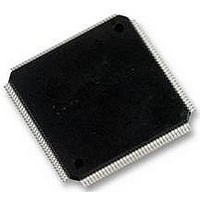
LPC2378FBD144 NXP Semiconductors, LPC2378FBD144 Datasheet - Page 12

LPC2378FBD144
Manufacturer Part Number
LPC2378FBD144
Description
MCU 32BIT ARM7, 10/100, USB, CAN
Manufacturer
NXP Semiconductors
Datasheet
1.LPC2378FBD144.pdf
(68 pages)
Specifications of LPC2378FBD144
Core Size
32bit
No. Of I/o's
104
Program Memory Size
512KB
Ram Memory Size
58KB
Cpu Speed
72MHz
Oscillator Type
External, Internal
No. Of Timers
4
No. Of Pwm Channels
6
Digital Ic Case
RoHS Compliant
Controller Family/series
LPC23xx
Rohs Compliant
Yes
Available stocks
Company
Part Number
Manufacturer
Quantity
Price
Company:
Part Number:
LPC2378FBD144
Manufacturer:
ST
Quantity:
43
Company:
Part Number:
LPC2378FBD144
Manufacturer:
NXP
Quantity:
5 000
Company:
Part Number:
LPC2378FBD144,551
Manufacturer:
ADI
Quantity:
2 397
Company:
Part Number:
LPC2378FBD144,551
Manufacturer:
NXP Semiconductors
Quantity:
10 000
NXP Semiconductors
Table 3.
LPC2377_78
Product data sheet
Symbol
P2[11]/EINT1/
MCIDAT1/
I2STX_CLK
P2[12]/EINT2/
MCIDAT2/
I2STX_WS
P2[13]/EINT3/
MCIDAT3/
I2STX_SDA
P3[0] to P3[31]
P3[0]/D0
P3[1]/D1
P3[2]/D2
P3[3]/D3
P3[4]/D4
P3[5]/D5
P3[6]/D6
P3[7]/D7
P3[23]/CAP0[0]/
PCAP1[0]
P3[24]/CAP0[1]/
PWM1[1]
Pin description
Pin
75
73
71
137
140
144
2
9
12
16
19
45
40
[1]
[1]
[6]
[6]
[6]
[1]
[1]
[1]
[1]
[1]
[1]
[1]
[1]
…continued
Type
I/O
I
O
I/O
I/O
I
O
I/O
I/O
I
O
I/O
I/O
I/O
I/O
I/O
I/O
I/O
I/O
I/O
I/O
I/O
I/O
I/O
I/O
I/O
I/O
I/O
I/O
I/O
I
I
I/O
I
O
Description
P2[11] — General purpose digital input/output pin.
EINT1 — External interrupt 1 input.
MCIDAT1 — Data line for SD/MMC interface.
I2STX_CLK — Transmit Clock. It is driven by the master and received by the slave.
Corresponds to the signal SCK in the I
P2[12] — General purpose digital input/output pin.
EINT2 — External interrupt 2 input.
MCIDAT2 — Data line for SD/MMC interface.
I2STX_WS — Transmit Word Select. It is driven by the master and received by the
slave. Corresponds to the signal WS in the I
P2[13] — General purpose digital input/output pin.
EINT3 — External interrupt 3 input.
MCIDAT3 — Data line for SD/MMC interface.
I2STX_SDA — Transmit data. It is driven by the transmitter and read by the
receiver. Corresponds to the signal SD in the I
Port 3: Port 3 is a 32 bit I/O port with individual direction controls for each bit. The
operation of port 3 pins depends upon the pin function selected via the pin connect
block. Pins 8 through 22, and 27 through 31 of this port are not available.
P3[0] — General purpose digital input/output pin.
D0 — External memory data line 0.
P3[1] — General purpose digital input/output pin.
D1 — External memory data line 1.
P3[2] — General purpose digital input/output pin.
D2 — External memory data line 2.
P3[3] — General purpose digital input/output pin.
D3 — External memory data line 3.
P3[4] — General purpose digital input/output pin.
D4 — External memory data line 4.
P3[5] — General purpose digital input/output pin.
D5 — External memory data line 5.
P3[6] — General purpose digital input/output pin.
D6 — External memory data line 6.
P3[7] — General purpose digital input/output pin.
D7 — External memory data line 7.
P3[23] — General purpose digital input/output pin.
CAP0[0] — Capture input for Timer 0, channel 0.
PCAP1[0] — Capture input for PWM1, channel 0.
P3[24] — General purpose digital input/output pin.
CAP0[1] — Capture input for Timer 0, channel 1.
PWM1[1] — Pulse Width Modulator 1, output 1.
All information provided in this document is subject to legal disclaimers.
Rev. 5 — 17 June 2010
Single-chip 16-bit/32-bit microcontrollers
2
S-bus specification.
2
S-bus specification.
2
S-bus specification.
LPC2377/78
© NXP B.V. 2010. All rights reserved.
12 of 68


