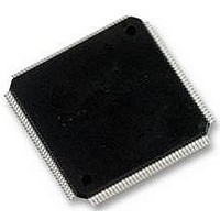
LPC2378FBD144 NXP Semiconductors, LPC2378FBD144 Datasheet - Page 8

LPC2378FBD144
Manufacturer Part Number
LPC2378FBD144
Description
MCU 32BIT ARM7, 10/100, USB, CAN
Manufacturer
NXP Semiconductors
Datasheet
1.LPC2378FBD144.pdf
(68 pages)
Specifications of LPC2378FBD144
Core Size
32bit
No. Of I/o's
104
Program Memory Size
512KB
Ram Memory Size
58KB
Cpu Speed
72MHz
Oscillator Type
External, Internal
No. Of Timers
4
No. Of Pwm Channels
6
Digital Ic Case
RoHS Compliant
Controller Family/series
LPC23xx
Rohs Compliant
Yes
Available stocks
Company
Part Number
Manufacturer
Quantity
Price
Company:
Part Number:
LPC2378FBD144
Manufacturer:
ST
Quantity:
43
Company:
Part Number:
LPC2378FBD144
Manufacturer:
NXP
Quantity:
5 000
Company:
Part Number:
LPC2378FBD144,551
Manufacturer:
ADI
Quantity:
2 397
Company:
Part Number:
LPC2378FBD144,551
Manufacturer:
NXP Semiconductors
Quantity:
10 000
NXP Semiconductors
Table 3.
LPC2377_78
Product data sheet
Symbol
P0[18]/DCD1/
MOSI0/MOSI
P0[19]/DSR1/
MCICLK/SDA1
P0[20]/DTR1/
MCICMD/SCL1
P0[21]/RI1/
MCIPWR/RD1
P0[22]/RTS1/
MCIDAT0/TD1
P0[23]/AD0[0]/
I2SRX_CLK/
CAP3[0]
P0[24]/AD0[1]/
I2SRX_WS/
CAP3[1]
P0[25]/AD0[2]/
I2SRX_SDA/
TXD3
P0[26]/AD0[3]/
AOUT/RXD3
P0[27]/SDA0
Pin description
Pin
86
85
83
82
80
13
11
10
8
35
[2]
[3]
[1]
[1]
[1]
[1]
[1]
[2]
[2]
[4]
…continued
Type
I/O
I
I/O
I/O
I/O
I
O
I/O
I/O
O
I
I/O
I/O
I
O
I
I/O
O
O
O
I/O
I
I/O
I
I/O
I
I/O
I
I/O
I
I/O
O
I/O
I
O
I
I/O
I/O
Description
P0[18] — General purpose digital input/output pin.
DCD1 — Data Carrier Detect input for UART1.
MOSI0 — Master Out Slave In for SSP0.
MOSI — Master Out Slave In for SPI.
P0[19] — General purpose digital input/output pin.
DSR1 — Data Set Ready input for UART1.
MCICLK — Clock output line for SD/MMC interface.
SDA1 — I
P0[20] — General purpose digital input/output pin.
DTR1 — Data Terminal Ready output for UART1.
MCICMD — Command line for SD/MMC interface.
SCL1 — I
P0[21] — General purpose digital input/output pin.
RI1 — Ring Indicator input for UART1.
MCIPWR — Power Supply Enable for external SD/MMC power supply.
RD1 — CAN1 receiver input. (LPC2378 only)
P0[22] — General purpose digital input/output pin.
RTS1 — Request to Send output for UART1.
MCIDAT0 — Data line for SD/MMC interface.
TD1 — CAN1 transmitter output. (LPC2378 only)
P0[23] — General purpose digital input/output pin.
AD0[0] — A/D converter 0, input 0.
I2SRX_CLK — Receive Clock. It is driven by the master and received by the slave.
Corresponds to the signal SCK in the I
CAP3[0] — Capture input for Timer 3, channel 0.
P0[24] — General purpose digital input/output pin.
AD0[1] — A/D converter 0, input 1.
I2SRX_WS — Receive Word Select. It is driven by the master and received by the
slave. Corresponds to the signal WS in the I
CAP3[1] — Capture input for Timer 3, channel 1.
P0[25] — General purpose digital input/output pin.
AD0[2] — A/D converter 0, input 2.
I2SRX_SDA — Receive data. It is driven by the transmitter and read by the
receiver. Corresponds to the signal SD in the I
TXD3 — Transmitter output for UART3.
P0[26] — General purpose digital input/output pin.
AD0[3] — A/D converter 0, input 3.
AOUT — D/A converter output.
RXD3 — Receiver input for UART3.
P0[27] — General purpose digital input/output pin. Output is open-drain.
SDA0 — I
All information provided in this document is subject to legal disclaimers.
2
2
2
C1 clock input/output (this is not an open-drain pin).
C1 data input/output (this is not an open-drain pin).
C0 data input/output. Open-drain output (for I
Rev. 5 — 17 June 2010
Single-chip 16-bit/32-bit microcontrollers
2
S-bus specification.
2
S-bus specification.
2
S-bus specification.
2
LPC2377/78
C-bus compliance).
© NXP B.V. 2010. All rights reserved.
8 of 68


